Technique for repairing salient point and memory by using laser

A laser repair and memory technology, which is applied in the fields of electrical solid-state devices, semiconductor devices, and semiconductor/solid-state device manufacturing, etc., can solve problems such as weakening, detection mark oxidation, metal layer 24 adhesion, and diffusion barriers.

Inactive Publication Date: 2003-12-24
UNITED MICROELECTRONICS CORP
View PDF0 Cites 2 Cited by
  • Summary
  • Abstract
  • Description
  • Claims
  • Application Information

AI Technical Summary

Problems solved by technology

[0006] Since the prior art is to perform the circuit test and the laser repair process first, it may affect the subsequent formation of the second dielectric layer 22 and the metal layer 24
First of all, the circuit testing procedure directly connects the probe pins to the bump pads 14, so a serious probing mark may be formed on the bump pads 14 surface, and subsequently formed on the bump pads 14 surface The step coverage of the metal layer 24 is very poor, which will cause the loss or weakening of the metal layer 24's adhesion and diffusion barrier function, thereby affecting product reliability.
In addition, when the metal interconnect (interconnect) system utilizes copper process technology and low dielectric constant material as the insulating layer between the metals, the circuit test procedure directly performed on the bump pad 14 may face failure due to excessive test force. Caused bare copper or insulation cracks and other problems
At the same time, the oxidation of the detection marks on the copper gasket after needle testing is also a difficult challenge.
[0007] Secondly, since the laser repair process carried out after completing the circuit test program will cut off part of the fuse structure 16, a plurality of trenches (trench) 27 with a larger aspect ratio (aspect ratio) are formed on the surface of the semiconductor chip 10. , which in turn may produce voids in the second dielectric layer 22 filled in later, affecting product reliability

Method used


Image

  • Technique for repairing salient point and memory by using laser
  • Technique for repairing salient point and memory by using laser
  • Technique for repairing salient point and memory by using laser

Examples


Embodiment Construction

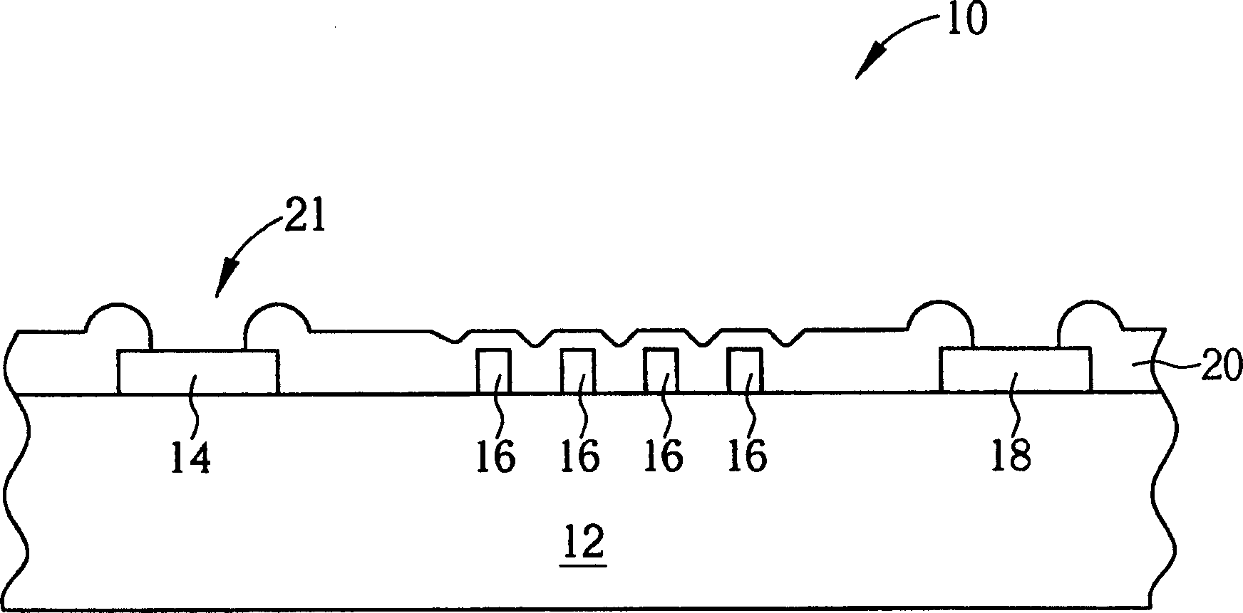
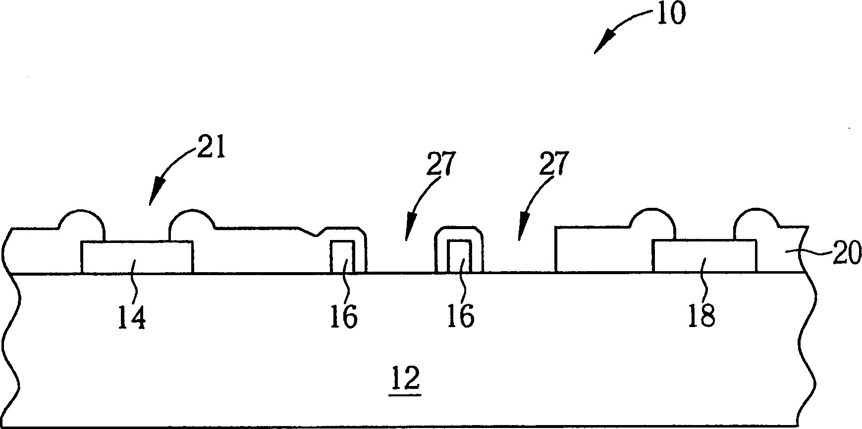
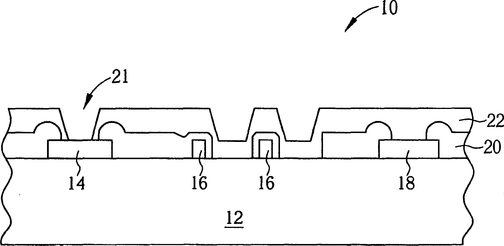
[0024] Please refer to Figure 5 to Figure 7 , Figure 5 to Figure 7 It is a schematic diagram of a first embodiment of performing a bump and memory laser repair process on a semiconductor chip 40 according to the present invention. Such as Figure 5 As shown, the semiconductor chip 40 includes a substrate 42 on which an integrated circuit region (not shown) is formed, and the integrated circuit region includes an embedded memory array. Wherein, the substrate 42 additionally includes a bump pad 44, a plurality of fuse structures 46 and an alignment key 48, and a silicon oxide layer (not shown) is formed on the The surface of the fuse structure 46 and the alignment structure 48 . The bump pads 44 are electrically connected to the integrated circuit region, so after the subsequent packaging process is completed, the integrated circuit can be electrically connected to external circuits through the bump pads 44 . In addition, the fuse structure 46 is formed on the upper layer ...


PUM


Abstract

First, the first dielectric layer is formed on the salient welding spot of the semiconductor chip. Next, the first dielectric layer is etched in order to form a contact hole and expose a part of the salient welding spot. Then, the second dielectric layer is formed on the surface outside the contact hole in the semiconductor chip. A metallization process is carried out for the bottom of the salient point in order to form a metal layer on the surface of the contact hole, and form a solder salient point on the metal layer. Finally, the procedure of laser-patching memory is completed.

Description

technical field [0001] The invention relates to a process of laser repairing (Laser Repair) of a memory after solder bumps are completed. Background technique [0002] In today's packaging technology, high-efficiency electronic components usually use solder balls or solder bumps to achieve the purpose of electrical and mechanical connection with each other. For example, an ultra large scale integration (ULSI) can use solder balls or solder bumps to form electrical connections with a circuit board or other second stage packaging substrate. Connection, this connection technology is called flip-chip packaging (Flip-chippackaging, FC). [0003] Please refer to Figure 1 to Figure 4 , Figure 1 to Figure 4 It is a schematic diagram of a conventional memory laser repair process on a semiconductor chip 10 . Such as figure 1 As shown, the semiconductor chip 10 includes a substrate 12 on which an integrated circuit region (not shown) is formed, and the int...

Claims


Application Information

Patent Timeline
Patent Type & Authority Applications(China)
IPC IPC(8): H01L21/60H01L21/768H01L21/82
CPCH01L2224/11
Inventor 陈国明刘洪民
Owner UNITED MICROELECTRONICS CORP
Why Eureka
Try Eureka