
Rapid energy transfer tempering device and method

A technology of energy transmission and tempering device, which is applied in the direction of electrical components, semiconductor/solid-state device manufacturing, circuits, etc., and can solve problems such as unstable energy density, high surface roughness and poor uniformity of polysilicon thin film layers

Inactive Publication Date: 2004-02-04
江雨龙
View PDF0 Cites 7 Cited by
  • Summary
  • Abstract
  • Description
  • Claims
  • Application Information

AI Technical Summary

Problems solved by technology

[0005] 1. Excimer laser tempering equipment is very expensive
[0006] 2. The energy density between one laser beam and another laser beam is often unstable
[0007] 3. Scanning tempering treatment of large-area substrates is time-consuming and labor-intensive
[0008] 4. Due to the growth and pushing effect between the crystallization regions (grains), some regions are raised and some regions are sunken, resulting in the absence of high surface roughness and poor uniformity of the polysilicon film layer
[0010] 1. Due to the low temperature (400°C-600°C), the growth rate of the individual crystallization regions of the polysilicon thin film layer produced by the tempering method of the furnace tube is slow, and the production capacity is limited
[0011] 2. Due to the low temperature (400°C-600°C), the energy provided is low, and the individual crystallization regions of the polysilicon film layer produced by the furnace tempering method are small, and the conductivity is lower than that of the polysilicon film produced by laser tempering. Floor
[0012] Another form of furnace tube tempering is a furnace tube tempering metal induced crystallization (metal induced crystallization) technology or metal induced lateral crystallization (metal induced lateral crystallization) technology, which is different from the furnace tube tempering solid phase crystallization technology in that A metal catalyst layer is deposited or vapor-deposited on or under the crystalline silicon thin film layer, which can reduce the furnace tube temperature and tempering time required for the transformation of the amorphous silicon thin film layer into polysilicon under the action of metal catalysis, but the furnace tube tempering metal induces The polysilicon film layer produced by crystallization or metal-induced lateral crystallization technology, in addition to the two disadvantages of furnace tempering solid phase crystallization technology, the phenomenon of metal atom diffusion (diffusion) will lead to pollution problems of metal residues in the polysilicon film layer

Method used


Image

  • Rapid energy transfer tempering device and method
  • Rapid energy transfer tempering device and method
  • Rapid energy transfer tempering device and method

Examples


Embodiment Construction

[0031] The present invention will be described below in conjunction with the accompanying drawings, and those skilled in the art should understand that the following description is only for illustration purposes, and is not intended to limit the present invention.

[0032] 【The first preferred embodiment】

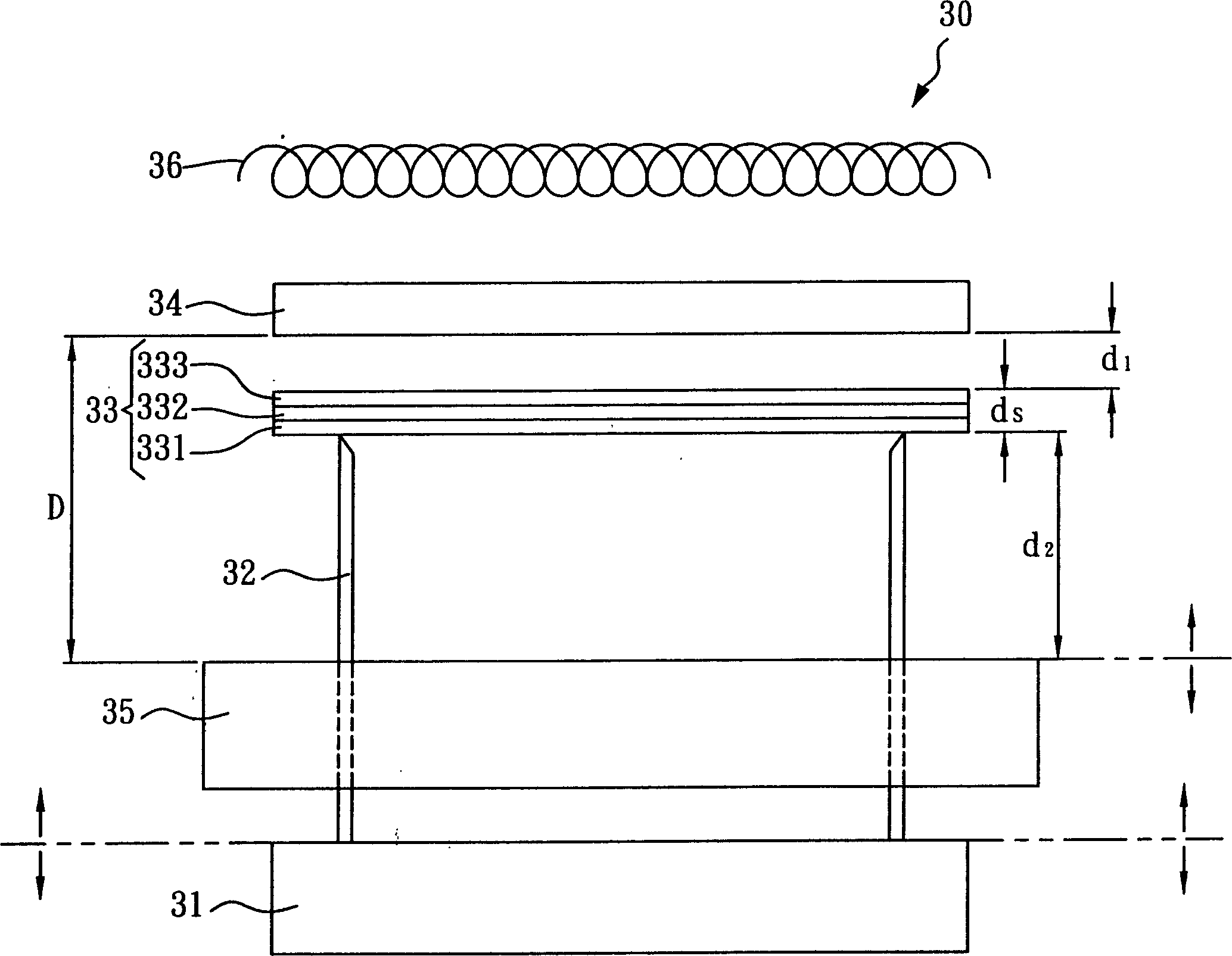
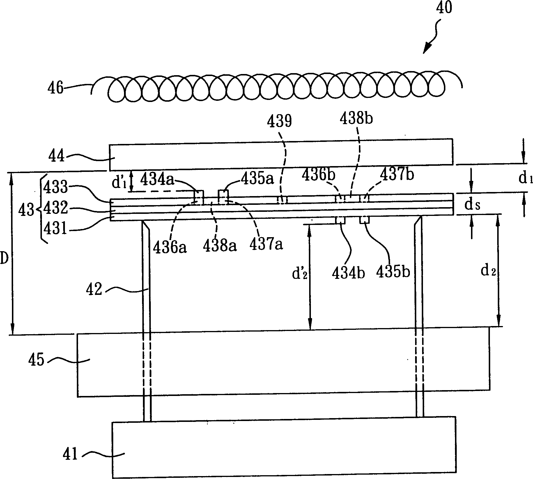
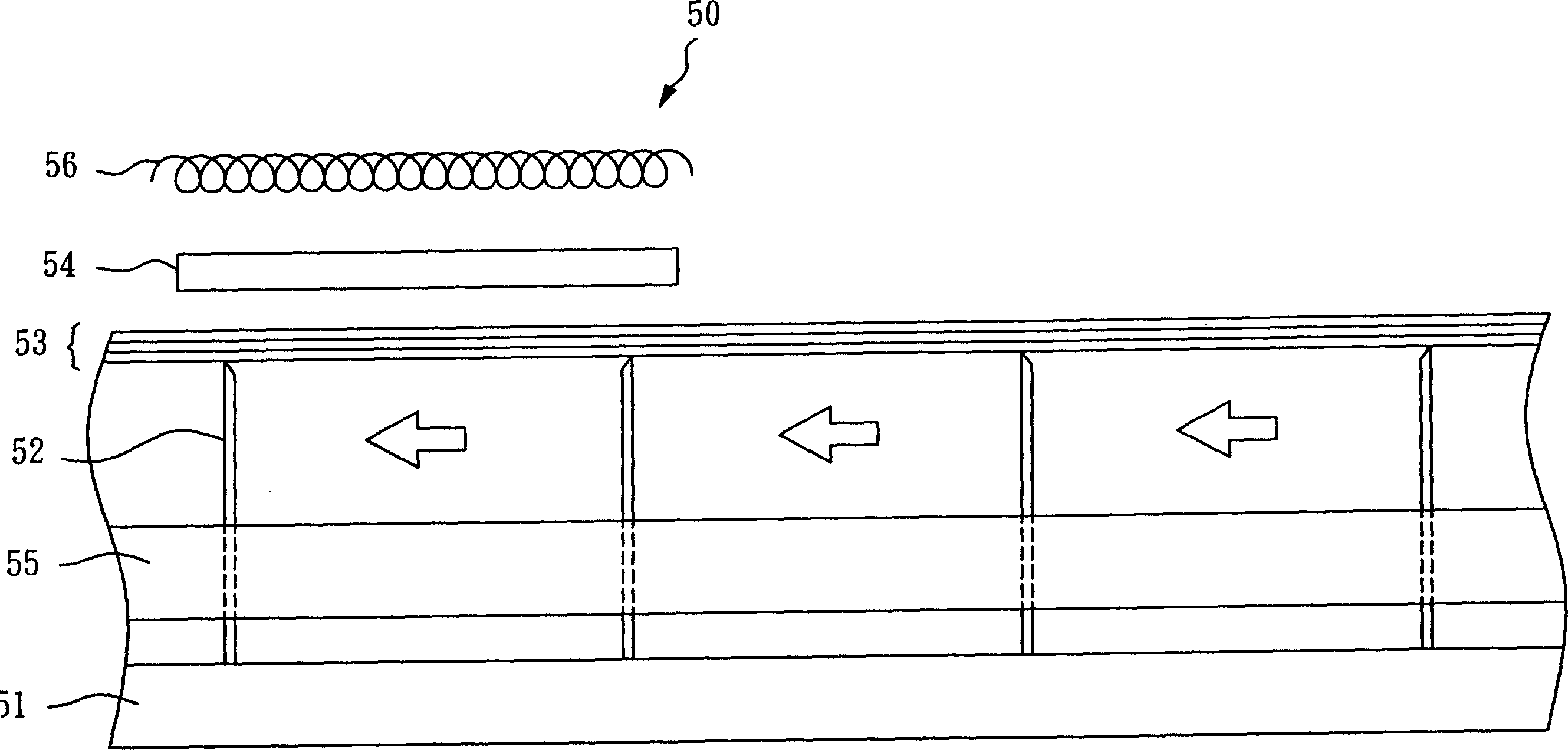
[0033] figure 1 It is a schematic diagram of the rapid energy transmission tempering device 30 of the first preferred embodiment of the present invention, including: a plurality of quartz columns 32 fixed on a carrier plate 31, a test piece 33 supported by a plurality of quartz columns 32 and having a thickness of dS , the test piece comprises a glass substrate 331, a silicon dioxide layer 332 and an amorphous silicon thin film layer 333 deposited sequentially on the glass substrate 331; an energy plate 34 is located at a first distance d1 above the test piece 33; A heat dissipation plate 35 is located at a second distance d2 below the test piece 33, allowing a plurality o...


PUM

PropertyMeasurementUnit
thicknessaaaaaaaaaa

Abstract

The method sets an energy plate between tungsten halogen or xenon arc lamp and a amorphous film deposited on a glass base plate to use heat energy released by amorphous film to heat it to be a polycrystal film. It also can be made by setting a heat radiating plate and a load plate at another side of glass base plate to control distance between them so as to control energy quantity transmission or setting a heat guiding layer and a heat isolation layer between glass base plate and polycrystal film, a heat radiating layer on anotherside of glass base plate and heat receiving layer on amorphous film to control heat guiding dirction for guiding growth direction of crystallization.

Description

(1) Technical field [0001] The invention relates to a rapid energy transmission tempering device and method. (2) Background technology [0002] Integrating thin-film transistor (TFT) driving elements and thin-film solar cells on a glass or a plastic substrate is a basic requirement for a new generation of thin-film transistor (TFT) flat-panel displays and thin-film solar cells. Due to low temperature polysilicon (LTPS for short) ) can be integrated on a glass or a plastic substrate, and because it has an electron mobility that is one to two orders of magnitude higher than that of amorphous silicon, it can effectively improve the characteristics of thin-film transistor drive elements. Low-temperature polysilicon has become a new generation of flat-panel displays. Thin-film transistor (TFT) driving components and important materials for thin-film solar cells. [0003] The polysilicon film part of the polysilicon (polysilicon) thin film transistor (TFT) panel of the thin film ...

Claims


Application Information

Patent Timeline
Patent Type & Authority Applications(China)
IPC IPC(8): H01L21/324
Inventor 江雨龙
Owner 江雨龙
Learn More