Method of manufacturing electronic part and electronic part obtained by the method

A technology of electronic components and production methods, which is applied in the direction of assembling printed circuits with electrical components, electrical components, and electrical solid devices, and can solve problems such as multi-time, narrow gaps between semiconductor chips and circuit boards, and increased costs

Inactive Publication Date: 2004-05-19
SUMITOMO BAKELITE CO LTD
View PDF1 Cites 16 Cited by
  • Summary
  • Abstract
  • Description
  • Claims
  • Application Information

AI Technical Summary

Problems solved by technology

However, according to this method, a heating step is necessary for the connection of each terminal and the curing of the resin, and the cost inevitably increases
And it takes a lot of time to pour the resin because the gap between the semiconductor chip and the circuit board is narrow

Method used


Image

  • Method of manufacturing electronic part and electronic part obtained by the method
  • Method of manufacturing electronic part and electronic part obtained by the method
  • Method of manufacturing electronic part and electronic part obtained by the method

Examples


Embodiment 1 and comparative Embodiment 1

[0110] (1) Preparation of Adhesive Varnish 1

[0111] To 104 g of methyl ethyl ketone were added 106 g of soluble cresol resin [manufactured by SUMITOMO DUREZ Co. Ltd.; PR-HF-3; hydroxyl equivalent weight of 106], 35 g of diallyl bisphenol A type epoxy resin [NIPPON KAYAKU Co. , Ltd. manufacture; RE-810NM; epoxy equivalent is 225], and 210 g of dicyclopentadiene type epoxy resin [NIPPON KAYAKU Co, Ltd. manufacture; XD-1000L; epoxy equivalent is 248], was dissolved , to make adhesive varnish 1 for metal bonding.

[0112] (2) Preparation of multilayer circuit board

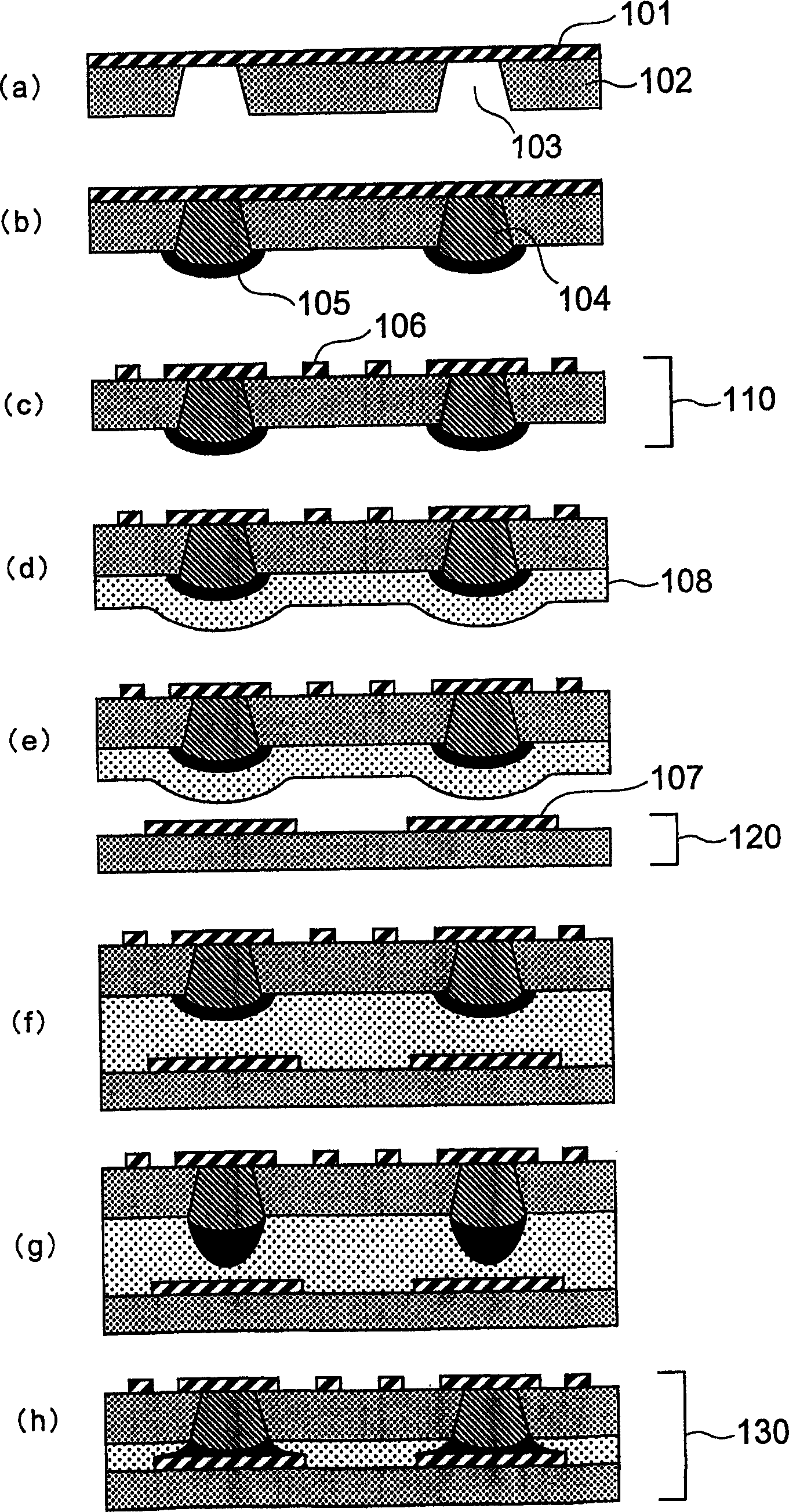
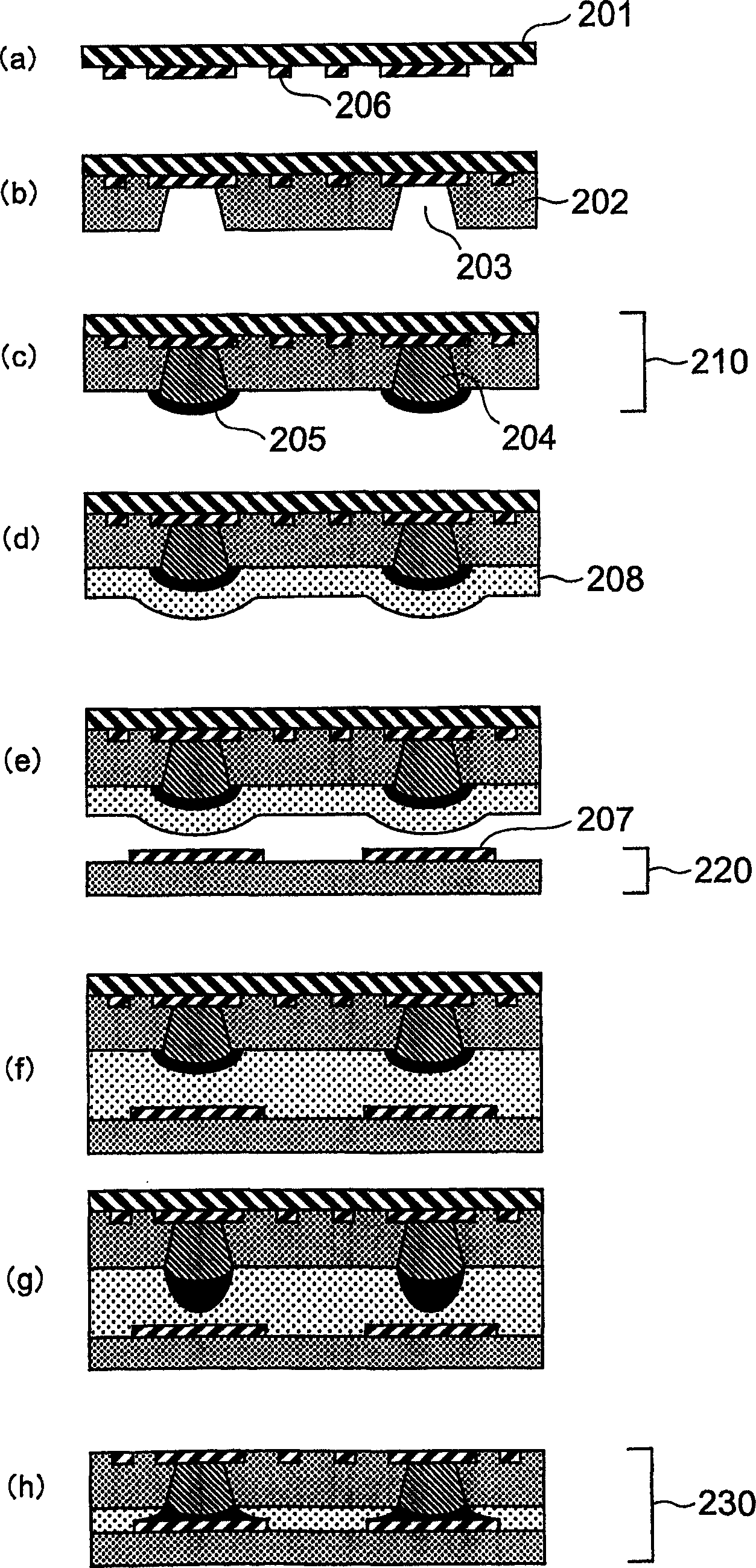
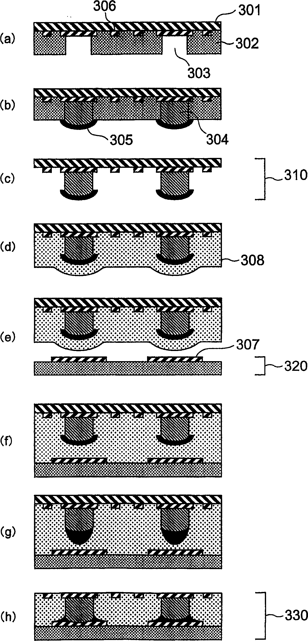
[0113] A polyimide resin insulating film on a flexible printed wiring board (SUMITOMO BAKELITE Co., Ltd.; manufactured by A1FLEC) includes a copper foil (metal foil 101; thickness: 18 μm) and a polyimide resin insulating film (insulating film 102; thickness: 25 µm), on which 300 through holes (via holes 103) were formed, each of which was formed by UV-YAG laser, with a top diameter of 45 µm and a bottom diameter o...

Embodiment 2

[0124] (1) Preparation of Adhesive Varnish 2

[0125] 106 g of soluble cresol resin [manufactured by SUMITOMO DUREZ Co. Ltd.;, PR-HF-3], 105 g of phenolphthalein [manufactured by TOKYO KASEI Co., Ltd.], and 405 g of diallyl were added to 165 g of methyl ethyl ketone. A bisphenol A type epoxy resin [manufactured by NIPPON KAYAKU Co, Ltd.; RE-810NM] was dissolved to prepare an adhesive varnish 2 for metal bonding.

[0126] (2) Preparation of multilayer circuit board

[0127] A polyimide resin insulating film on a flexible printed wiring board (SUMITOMO BAKELITE Co., Ltd.; manufactured by A1FLEC) comprising a copper foil (metal foil 101; thickness: 18 μm) and a polyimide resin insulating film (insulating film 102; thickness: 25 µm), on which 300 through holes (via holes 103) were formed, each of which was formed by UV-YAG laser, with a top diameter of 45 µm and a bottom diameter of 25 µm. After the inner and outer parts of the hole are cleaned with a resin etching solution cont...


PUM


Abstract

In a process for producing an electronic part which comprises soldering (A) an electronic member having conductor portions I for electric connection having a solder layer or a solder bump (a solder portion) on a surface of a tip and (B) an electronic member to be connected having conductor portions II for electric connection arranged at positions corresponding to positions of conductor portions I by pressing (A) to (B) under heating via an adhesive layer, the solder portion is brought into contact with the adhesive layer, the solder portion is melted by heating at a temperature of or higher than a melting point of the solder, the soldering is conducted by pressing the melted solder portion, and the adhesive layer is cured. An electronic part is obtained in accordance with the process. Electric connection is surely achieved and a highly reliable electronic part can be obtained with excellent productivity.

Description

technical field [0001] The present invention relates to a production method of an electronic component and an electronic component produced by the method. More specifically, the present invention relates to a production method of a high-reliability multilayer circuit board in which the connection between layers is ensured at high Successfully realized at low production efficiency, and also relates to a production method of a high-reliability semiconductor device with high production efficiency, which is accomplished by efficiently mounting a semiconductor flip-chip on a wiring substrate by a no-flow underfill method, and It relates to a multilayer circuit board and a semiconductor device obtained by the above method. Background technique [0002] Recently, while electronic instruments provide stronger functions, they are lighter in weight, smaller in volume, higher in integration of electronic components, and are assembled in higher density on electronic instruments. Semic...

Claims


Application Information

Patent Timeline
Patent Type & Authority Applications(China)
IPC IPC(8): H01L21/48H01L21/56H01L21/60H01L21/68H01L23/29H01L23/498H05K3/20H05K3/30H05K3/34H05K3/38H05K3/46
CPCH01L2224/16227H05K2203/1189H01L24/29H05K2201/0195H01L2224/81801H01L2924/01039H01L2224/16H01L2924/01015H01L2924/01087H01L2924/01004H01L2924/0132H01L2924/01059H01L2924/01078H05K2201/10977H01L2224/73203H01L23/293H01L2221/68345H01L2224/16237H01L2924/01005H01L21/486H05K2203/0475H01L2224/2919H01L2924/01013H01L21/563H01L2924/01322H05K3/20H01L2224/29111H05K3/4617H01L2224/13111H01L2924/01051H01L2924/01027H05K2201/0394H05K3/305H01L2224/32225H01L2924/0105H05K3/3436H01L2224/81191H01L2924/01025H01L2924/01327H01L2924/01047H01L2224/16225H01L2224/1147H01L2924/01046H01L2924/01006H01L2924/01072H01L21/6835H01L2924/01079H01L2924/01074H05K3/386H01L2924/1579H01L2224/83192H01L2924/0103H01L2924/01082H01L2224/73204H05K3/3489H01L2924/014H01L2924/01029H01L2924/01019H01L2924/01033H01L23/49827H01L2924/01075H01L24/81H01L2224/05571H01L2224/05573H01L2224/73104H01L2924/00014H01L2924/12042Y02P70/50H01L2924/00015H01L2924/3512H01L2924/00H01L2224/05599
Inventor 冈田亮一青木仁奥川良隆中村谦介伊藤真一郎
Owner SUMITOMO BAKELITE CO LTD
Why Eureka
Try Eureka