Super-thin copper foil with carrier, its mfg. method and printed wiring base plate

A technology of ultra-thin copper foil and manufacturing method, which is applied in the manufacture of printed circuit precursors, printed circuits, printed circuit manufacturing, etc., and can solve the problems of copper foil fracture, easy wrinkles and creases, and low mechanical strength of thin copper foil

Inactive Publication Date: 2004-05-26
FURUKAWA ELECTRIC CO LTD
View PDF1 Cites 22 Cited by
  • Summary
  • Abstract
  • Description
  • Claims
  • Application Information

AI Technical Summary

Problems solved by technology

[0007] However, thin copper foil (ultra-thin copper foil) has low mechanical strength, and it is prone to wrinkles and creases when manufacturing printed wiring boards, and sometimes copper foil breaks, so it has begun to be used as ultra-thin copper foil for precision graphics applications. The ultra-thin copper foil with carrier is used to directly deposit the ultra-thin copper foil layer on one side of the carrier copper foil through the peeling layer

Method used


Image

  • Super-thin copper foil with carrier, its mfg. method and printed wiring base plate
  • Super-thin copper foil with carrier, its mfg. method and printed wiring base plate
  • Super-thin copper foil with carrier, its mfg. method and printed wiring base plate

Examples


Embodiment 1

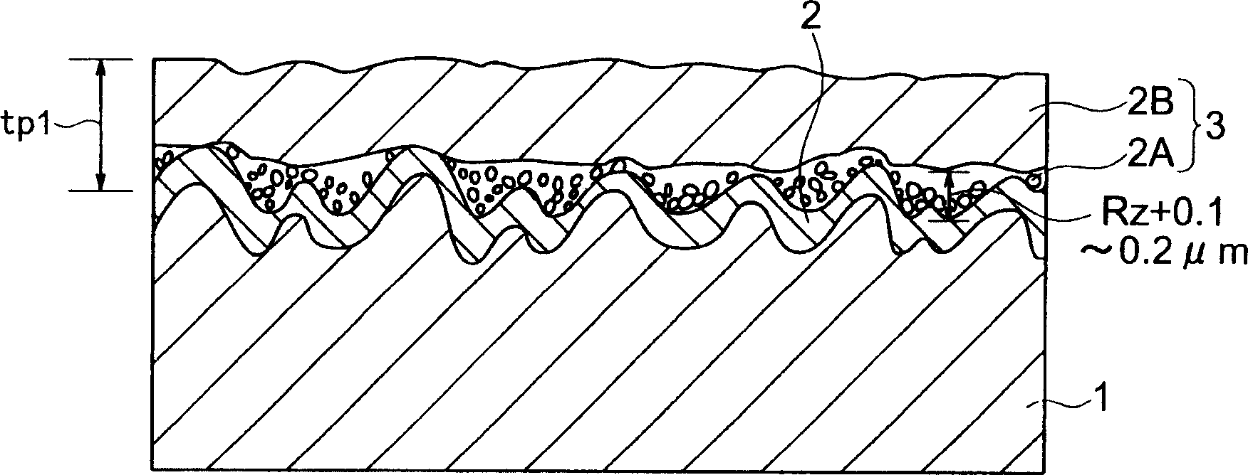
[0063] Example 1 ( figure 1 )

[0064] 1. Preparation of carrier copper foil: As carrier copper foil 1, an untreated electrolytic copper foil with a thickness of 31 μm and a gloss surface roughness Rz=1.5 μm was prepared.

[0065] 2. Forming a peeling layer: Continuously conduct electrical treatment on the glossy surface of the carrier copper foil 1 to form a metal Cr adhesion amount of 0.50mg / dm 2 Metallic chrome peel off layer 2.

[0066] 3. Form a strike plating layer containing P on the surface of the peeling layer 2 and its vicinity: then on the peeling layer 2,

[0067] Cu 2 P 2 o 7 ·3H 2 O: 30g / L

[0068] K 4 P 2 o 7 : 300g / L

[0069] pH: 8

[0070] Current density in solution: 1.5A / dm 2 Strike plating was performed for 30 seconds under the conditions of , and a P-containing layer 2A was formed on the surface of the release layer and its vicinity.

[0071] 4. Form extremely thin copper foil: then on the strike plating layer 2A containing P, on...

Embodiment 2

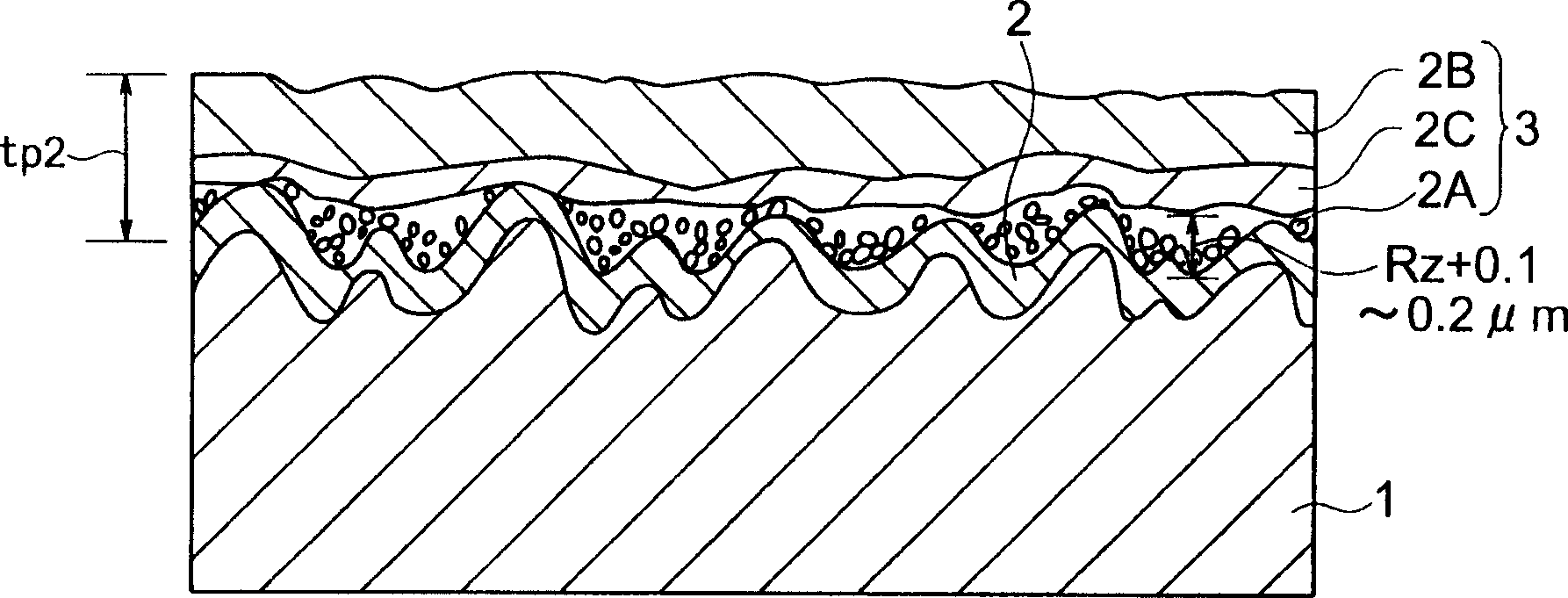
[0077] Example 2 ( figure 2 )

[0078] 1. Preparation of carrier copper foil: As carrier copper foil 1, an untreated electrolytic copper foil with a thickness of 31 μm and a gloss surface roughness Rz=0.2 μm was prepared.

[0079] 2. Forming a peeling layer: Continuously conduct electrical treatment on the glossy surface of the carrier copper foil 1 to form a layer with a Cr adhesion of 0.30 mg / dm 2 The release layer 2 is composed of a hydrated oxide film.

[0080] 3. Form a strike plating layer containing P on the surface of the peeling layer 2 and its vicinity: then on the peeling layer 2,

[0081] Cu 2 P 2 o 7 ·3H 2 O: 30g / L

[0082] K 4 P 2 o 7 : 300g / L

[0083] Current density: 1.5A / dm in solution of pH: 8 2 Strike plating was performed for 60 seconds under the same conditions to form a P-containing layer 2A on the surface of the release layer 2 and its vicinity.

[0084] 4. Forming ultra-thin copper foil-1: Then use it on the strike plating ...

Embodiment 3

[0094] Embodiment 3 ( figure 2 )

[0095] 1. Preparation of carrier copper foil: As carrier copper foil 1, an untreated electrolytic copper foil with a thickness of 35 μm and a gloss surface roughness Rz=0.8 μm was prepared.

[0096] 2. Forming a peeling layer: Continuously conduct electrical treatment on the glossy surface of the carrier copper foil 1 to form a layer with a metal adhesion of 0.50 mg / dm 2 The release layer 2 is composed of metal chromium and hydrated oxide film.

[0097] 3. Form a layer containing P on the surface of the peeling layer 2 and its vicinity: then on the peeling layer,

[0098] Cu 2 P 2 o 7 ·3H 2 O : 16g / L

[0099] K 4 P 2 o 7 : 300g / L

[0100] Current density: 1.5A / dm in solution of pH: 8 2 Strike plating was performed for 60 seconds under the same conditions to form a P-containing layer 2A on the surface of the release layer 2 and its vicinity.

[0101] 4. Forming an extremely thin copper layer-1: Then use it on the str...


PUM

PropertyMeasurementUnit
surface roughnessaaaaaaaaaa
peel strengthaaaaaaaaaa
Adhesion amountaaaaaaaaaa

Abstract

An ultra-thin copper foil with a carrier having a peeling layer able to withstand even high temperature working in the case of using a high heat resistant resin, enabling the carrier foil and the ultra-thin copper foil to be easily peeled apart, and reduced in the number of pinholes by uniform plating without impairing the peelability of the peeling layer, that is, an ultra-thin copper foil with a carrier comprised of a carrier foil, a peeling layer, and an ultra-thin copper foil, wherein the peeling layer and the ultra-thin copper foil are provided between them with a strike plating layer at the surface on the peeling layer side, an ultra-thin layer of copper is provided on this according to need, and an ultra-thin copper foil comprised of copper or a copper alloy or a phosphorus-containing copper or phosphorus-containing copper alloy is provided. The peeling layer between the carrier foil and the ultra-thin copper foil is chromium, a chromium alloy, a chromium-containing oxide hydrate layer, nickel, iron, or an alloy layer of the same or an oxide hydrate layer of the same.

Description

technical field [0001] The present invention relates to an ultra-thin copper foil with a carrier and a method for manufacturing the ultra-thin copper foil with a carrier, and particularly relates to a tape carrier suitable as a printed wiring board for high-density ultra-fine wiring (precise pattern) Very thin copper foil. Background technique [0002] The printed wiring board was produced as follows. First, on the surface of an electrically insulating substrate made of glass, epoxy resin, glass, polyimide resin, etc., a thin copper foil for forming a surface circuit is placed, and then heated and pressurized to manufacture a copper-clad laminate. [0003] Next, on the copper-clad laminate, through-hole drilling and through-hole electroplating are carried out in sequence, and then the copper foil on the surface of the copper-clad laminate is etched to form a desired line width and a desired line spacing. The wiring pattern, finally, undergoes solder resist formation and ot...

Claims


Application Information

Patent Timeline
Patent Type & Authority Applications(China)
IPC IPC(8): H05K1/09C25D1/04C25D1/22C25D5/10H05K3/02H05K3/38
CPCY10T428/12438Y10T428/12847C25D1/04H05K3/384C25D1/22Y10T428/12771C25D5/10Y10T428/12806Y10T428/12514Y10T428/12493Y10T428/1291Y10T428/12472H05K3/025C25D5/611H05K1/09
Inventor 铃木裕二松田晃
Owner FURUKAWA ELECTRIC CO LTD
Why Eureka
Try Eureka