
Bidirectional-light silicon controlled chip

A technology of silicon chip and two-way light, which is applied in the direction of electrical components, thyristors, electronic switches, etc., can solve the problem that the main silicon 4 cannot be cancelled, etc.

Inactive Publication Date: 2004-06-30
SHARP KK
View PDF0 Cites 8 Cited by
  • Summary
  • Abstract
  • Description
  • Claims
  • Application Information

AI Technical Summary

Problems solved by technology

However, there is a problem that the main thyristor 4 cannot be eliminated, because in the above case, the rectification characteristic Icom required for the triac 2 is not less than about 200 mArms, and in Figure 11 In the shown triac 2, a malfunction due to rectification failure usually exhibits a rectification characteristic Icom of about one-fifth of this value

Method used


Image

  • Bidirectional-light silicon controlled chip
  • Bidirectional-light silicon controlled chip
  • Bidirectional-light silicon controlled chip

Examples


no. 1 example

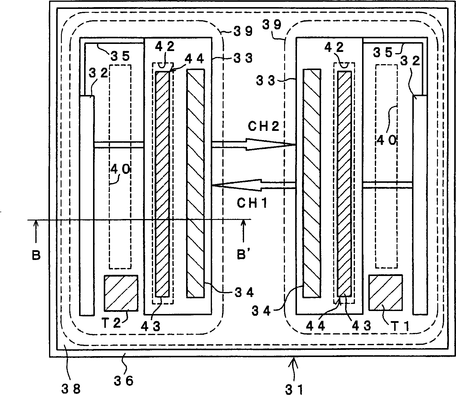
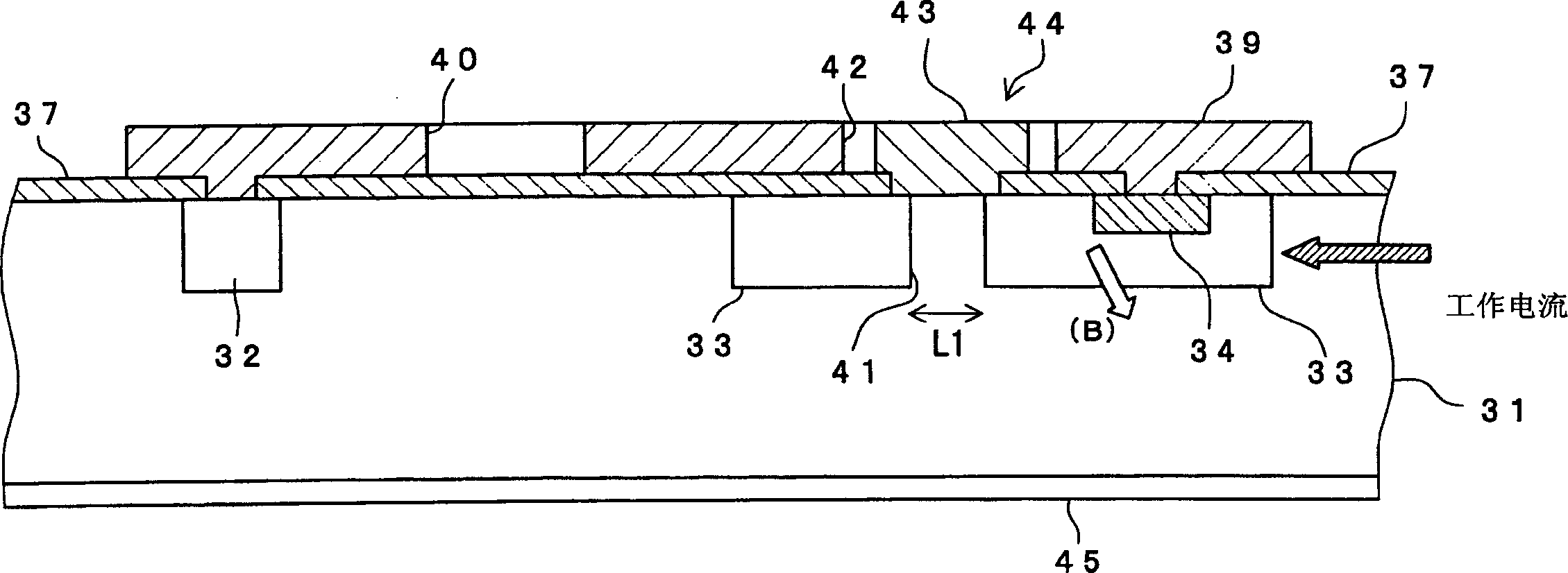
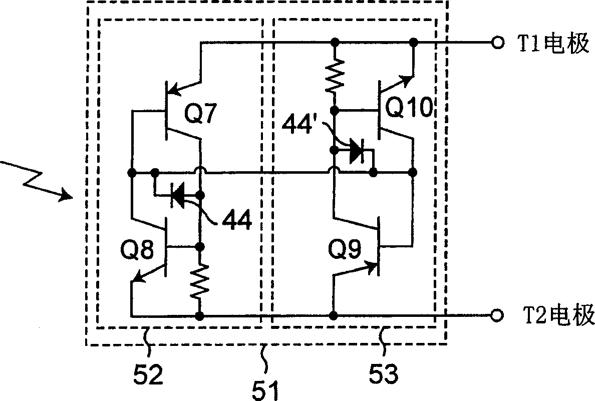
[0060] figure 1 A schematic diagram arrangement of the bidirectional phototriac chip of the present embodiment is shown. figure 2 is along figure 1 A cross-sectional view taken along the arrow B-B'. image 3 It is the equivalent circuit diagram of the bidirectional phototriac chip of this embodiment. Please note that the graphic arrangement of this phototriac chip is basically the same as Figure 11 The same as shown for the conventional triac 2.

[0061] The structure of the bidirectional phototriac chip is as follows: that is, two anode diffusion regions (P-type) 32 and two P gate diffusion regions (P-type) 33 opposite to them are symmetrically arranged with a horizontal flip axis in the figure On the front side of the N-type silicon substrate 31 . A cathode diffusion region (N type) 34 is provided on the side opposite to the anode diffusion region 32 in each P gate diffusion region 33 . Thus, a PNPN portion is formed extending from the anode diffusion region 22 on ...

no. 2 example

[0080] In the bidirectional phototriac substrate in the first embodiment, the working current regions of CH1 and CH2 cross each other, which can be clearly seen from their pattern layout. Therefore, the advantage of this chip is that the size of the chip can be reduced and the design is compact. But in turn, because the working currents of CH1 and CH2 cross each other, carrier interference will occur, although the injection of minority carriers (holes) into the N-type silicon substrate 31 is limited, and the number of residual carriers is reduced , but the rectification characteristic Icom is relatively low (drop). Therefore, in this embodiment, a bidirectional phototriac whose rectification characteristic Icom is further improved will be introduced.

[0081] Figure 4 A schematic pattern layout of the triac of this embodiment is shown. Although not shown Figure 4 sectional views and equivalent circuit diagrams, but they are basically similar to figure 2 and image 3 ....

no. 3 example

[0091] In the bidirectional phototriac chip of the second embodiment, the diffusion regions are arranged along two opposite sides of the chip periphery. Thus, the region in which the trench isolation region 70 is formed is a confinement region in the center portion, and CH1 and CH2 cannot be formed completely apart from each other. Thus, the rectification characteristic Icom cannot be sufficiently improved.

[0092] Furthermore, as described above, the lengths of the anode diffusion region, P gate diffusion region, and cathode diffusion region on the CH1 and CH2 sides are all shorter than in the case of the triac chip of the first embodiment. Therefore, due to the relatively short length of the diffusion region, the on-state voltage VT becomes very high, and the heat generation of the device increases.

[0093] Correspondingly, in this embodiment, a bidirectional phototriac chip capable of improving device characteristics and further improving rectification characteristics Ic...


PUM


Abstract

In a CH1 side photothyristor and a CH2 side photothyristor, a shot key barrier diode 44 is formed between a p-gate diffusion region 33 and an n-type silicon substrate 31. Accordingly, the pouring of a minority carrier from the p-gate diffusion region 33 into the n-type silicon substrate 31 is suppressed and the mount of remaining carrier is decreased whereby an excessive carrier remaining in the n-type silicon substrate 31 upon commutation reduces a chance to move toward a reverse channel side, thereby permitting the improvement of the commutation characteristics. Further, a light spot arc coupler for controlling the light spot arc and a load can be provided by combining with an LED.

Description

Background of the invention [0001] The present invention relates to a two-way light thyristor chip. [0002] Generally, as a solid state relay (hereinafter abbreviated as SSR) used with alternating current, there is one such as Figure 9 The circuit configuration shown. This SSR 8 is made up of the following components and parts: a phototrigger coupler 3, it is made up of light-emitting device 1 such as a LED (light-emitting diode) and so on and a triac 2 for triggering; The bidirectional thyristor (hereinafter sometimes referred to as the main thyristor) 4 used to control the load, and the shock absorber circuit composed of the resistor 5 and the capacitor 6, etc. [0003] The equivalent circuit diagram of the optical trigger coupler 3 constituting the SSR8 is shown in Figure 10 . The bidirectional phototriac 2 is composed of a phototriac 9 of CH (channel) 1 and a phototriac 10 of CH2. The phototriac 9 of CH1 is formed by connecting the base of a PNP transistor Q1 to the...

Claims


Application Information

Patent Timeline
Patent Type & Authority Applications(China)
IPC IPC(8): H01L29/47H01L29/74H01L29/747H01L29/872H01L31/0328H01L31/111
CPCH03K17/79H01L31/1113H03K17/74H03K17/04H03K17/7955
Inventor 鞠山满久保胜
Owner SHARP KK
Learn More