Two dimension photon crystal light swith having defect state and its application

A two-dimensional photonic crystal and defect state technology, applied in optics, nonlinear optics, instruments, etc., can solve problems such as difficult adjustment, difficult arrangement, and difficult realization, and achieve the effects of simple steps, wide application range, and easy manufacture

Inactive Publication Date: 2004-07-21
INST OF PHYSICS - CHINESE ACAD OF SCI
View PDF0 Cites 25 Cited by
  • Summary
  • Abstract
  • Description
  • Claims
  • Application Information

AI Technical Summary

Problems solved by technology

However, the optical switch manufactured by using the photonic bandgap shift mechanism is easy to cause pulse deformation due to the large group velocity dispersion at the band edge
Moreover, since it is difficult to fabricate photonic crystals with sharp band edges, the efficiency of optical switches fabricated by the mechanism of photonic bandgap shift is not high.
Usually, people use the introduction of defect states in the photonic bandgap, and use the movement of defect states to realize optical switches (document 6, ShengLAN, SatoshiNISHIKAWA, HiroshiISHIKAWA, and OsamuWADA,"Engineering PhotonicCrystal Impurity Bands for Waveguides, All-Optical Switches and Optical DalayLines" , Ieice Trans.electron., 2002, E85-c(1): 181-189; Literature 7, Sheng Lan, SatoshiNishikawa, and Osamu Wada, "Leverging deep photonic band gaps in photonic crystalimpurity bands", Appl.Phys.Lett.2001 , 78(15): 2101-2103), using semiconductor materials to prepare one-dimensional photonic crystals through epitaxial growth technology, introducing defects through different thicknesses of grown materials, and using the movement of defects in the band gap of photonic crystals to realize photonic crystal optical switches , but this method has great defects: first, the preparation process of photonic crystals is very complicated, difficult to control, and the deviation caused by manufacturing is relatively large, making it difficult to prepare ideal photonic crystals; second, the energy of light transmission is in other Diffraction in 2D causes energy loss, making it inefficient
In addition, through the coupling of defect states (document 8 Sheng Lan and Hiroshi Ishikawa, "Coupling of defect pairs and generation of dynamical band gaps in the impurity bands of nonlinear photonic custals for all-optical switching", Journal of Applied Physics", 2002, 91(5 ): 2573-2577) to realize the optical switch, the pillars are arranged periodically to prepare photonic crystals, but due to the small size of the pillars, it is very difficult to arrange, and it is difficult to find the same frequency but field distribution when selecting defect states different modes, therefore, it is experimentally difficult to achieve
This greatly limits the practical application of photonic crystal optical switches

Method used


Image

  • Two dimension photon crystal light swith having defect state and its application
  • Two dimension photon crystal light swith having defect state and its application
  • Two dimension photon crystal light swith having defect state and its application

Examples


Embodiment 1

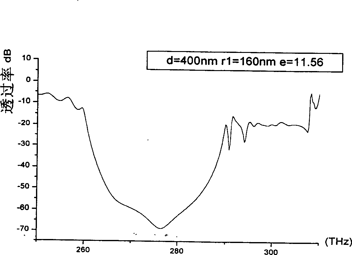
[0050] Example 1: In the infrared band, the movement of the defect state of the photonic crystal is used to realize the optical switch function of the two-dimensional photonic crystal

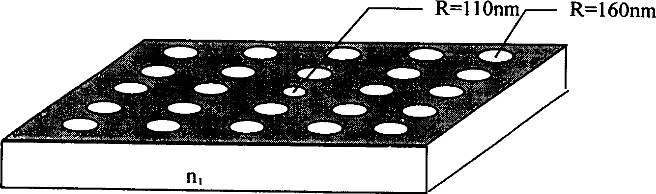
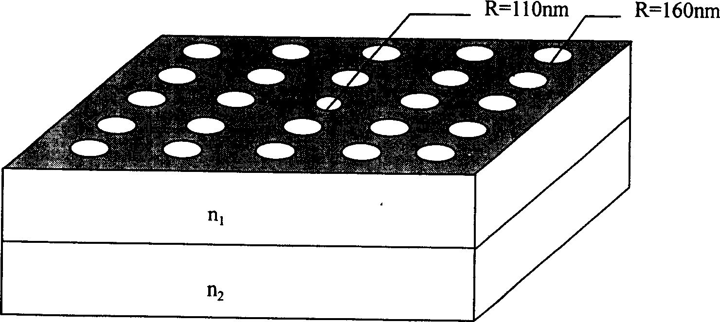
[0051] 1) Selection of materials

[0052] Choose GaAs (n=3.4) material with high refractive index. The high refractive index can increase the width and depth of the band gap of the photonic crystal, thereby making a high-quality photonic crystal and realizing a high-efficiency optical switch. GaAs has a high third-order nonlinear polarizability (n 2 =-4.1×10 -13 cm 2 / W, Shi Wangzhou, "Nano-GaAs embedded in SiO 2 Research on the preparation, structure and optical properties of thin films in the medium", N91525, P51, Chinese Academy of Sciences Literature Information Center), the refractive index can be changed with a smaller light intensity, so that the defect mode has a larger Move to realize high-efficiency optical switch.

[0053] 2) Preparation of samples.

[0054] Step 1: Use a material with a...


PUM

PropertyMeasurementUnit
refractive indexaaaaaaaaaa

Abstract

The present invention applies microprocessing technique to utilize high refractive index of semiconductor material to prepare high quality of two-dimensional photon crystal with defect state and optical switch can be realized by utilizing high third order-nonlinear polarizability and quick response time of semiconductor material. The produced optical switch can be widely used in field of optical communication and optical computer.

Description

Technical field [0001] The invention relates to an application technology using photonic crystals, in particular to a two-dimensional photonic crystal optical switch with defect states and applications thereof. Background technique [0002] Photonic crystals are an important basis for the preparation of integrated photonic devices. The optical switch prepared by using photonic crystals can be used as an optical multiplexer, optical regenerator, and applied to an optical sampling system. It can control the light transmission process very effectively. Therefore, it is very useful in the fields of optical computing and optical information processing. Important applications. However, the realization of optical switches requires high-quality photonic crystals, and the requirements for photonic band gaps are more stringent. Therefore, due to the limitation of photonic crystal preparation technology, there have been no experimental research reports on three-dimensional photonic crystal ...

Claims


Application Information

Patent Timeline
Patent Type & Authority Applications(China)
IPC IPC(8): G02F1/015
Inventor 刘元好胡小永王义全韩守振程丙英张道中
Owner INST OF PHYSICS - CHINESE ACAD OF SCI
Why Eureka
Try Eureka