
Method for preparing low dielectric films

A technology of low dielectric constant and hydrogenated silicon, which is applied in the direction of circuits, electrical components, electrical solid devices, etc., can solve the problem of high dielectric constant

Inactive Publication Date: 2004-08-18
POSTECH ACAD IND FOUND
View PDF2 Cites 15 Cited by
  • Summary
  • Abstract
  • Description
  • Claims
  • Application Information

AI Technical Summary

Problems solved by technology

However, the dielectric constant of the film disclosed in this patent is still high (3.3 to 4.0)

Method used


Image

  • Method for preparing low dielectric films
  • Method for preparing low dielectric films
  • Method for preparing low dielectric films

Examples


Embodiment 1

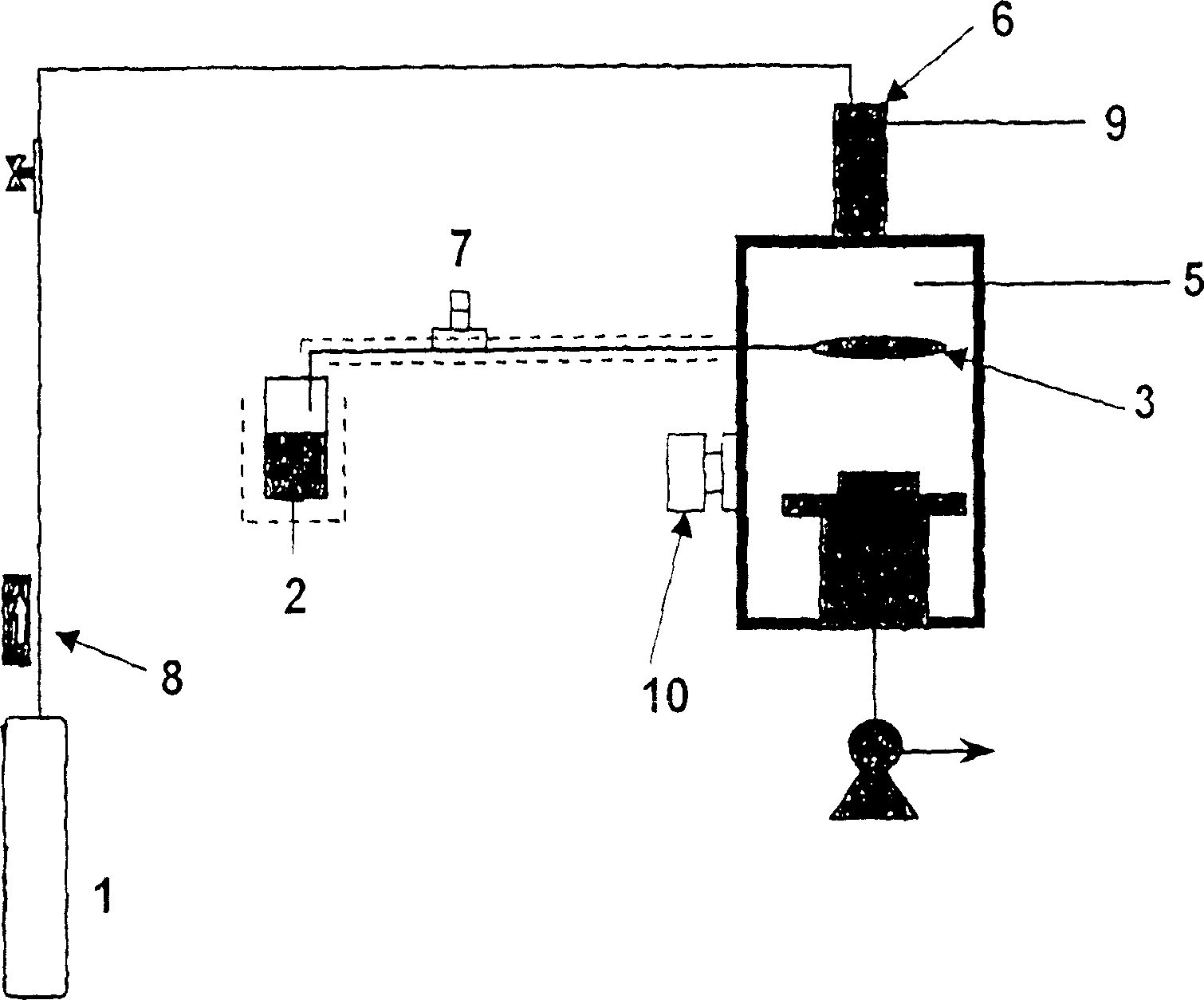
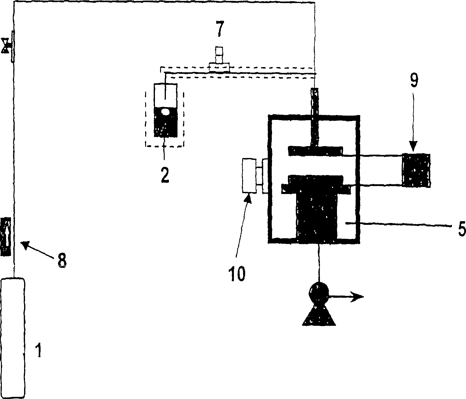
[0047] exist Figure 1b In the direct plasma device shown, vinyltrimethylsilane (VTMS, SiC 5 h 12 ) and O 2 SiCOH films were deposited on Pt substrates. During film deposition, O 2 The flow ratio of / VTMS was varied in the range of 1 to 13.3. The pressure and temperature in the reactor were 1 mmHg and 30°C, respectively, and the applied plasma power was 60W. The film thus deposited is annealed at a temperature of 300 to 500° C. under an argon atmosphere to obtain a film with a low dielectric constant.

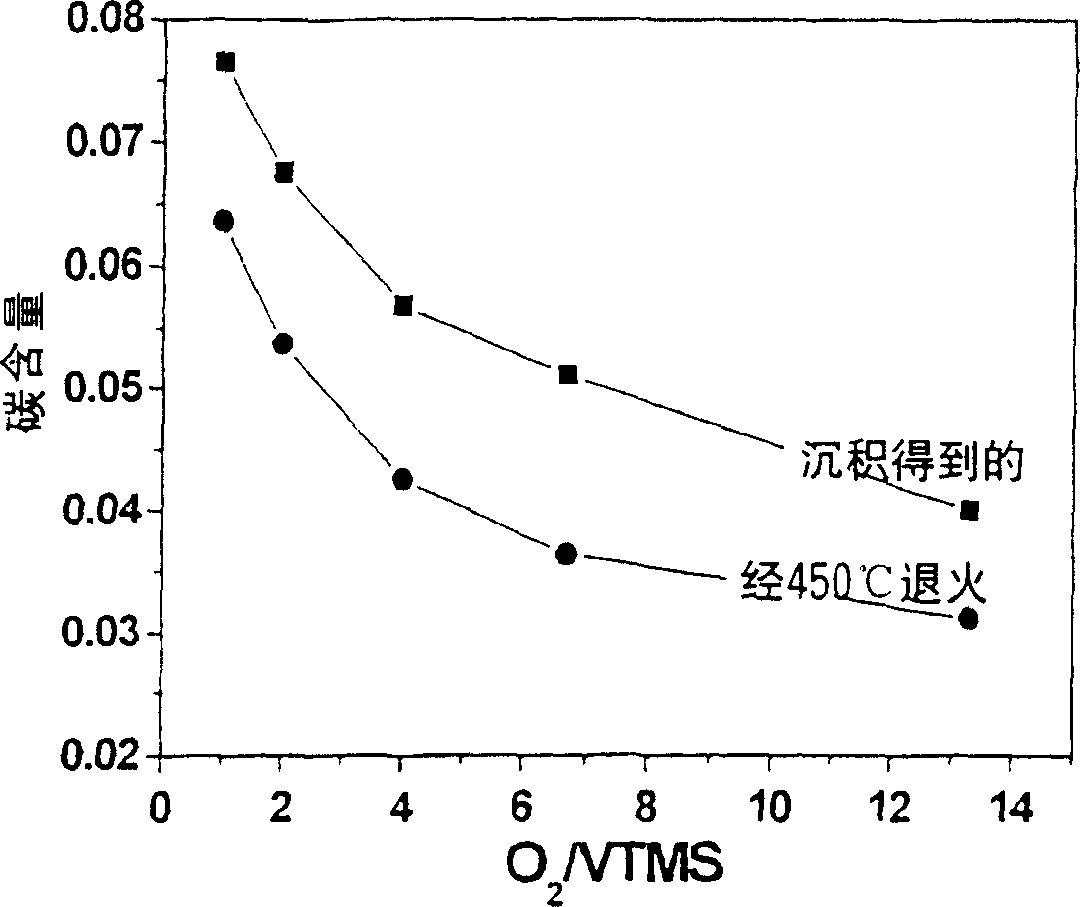
[0048] Such as figure 2 As shown, the corresponding carbon content of the as-deposited film and the film annealed at 450 °C increased with O 2 / VTMS flow ratio increases and decreases. image 3 The films annealed at 450° C. were shown to have a dielectric constant of 1.8 to 2.4, while the film deposited without annealing had a dielectric constant of 2.3 to 2.8. Figure 4 and 5 displayed on O 2 When the / VTMS flow ratio is 2, the dielectric constant of the film obtai...

Embodiment 2

[0052] Repeat the step of embodiment 1, difference is to use tetramethylsilane (4MS, SiC 4 h 12 ) and C 2 f 4 A mixture of VTMS (1:1) was used instead of VTMS to obtain a deposited film, which was subsequently annealed.

[0053] Figure 6 and Figure 7 The carbon content and dielectric constant of the as-deposited and annealed films are shown, respectively. The dielectric constant of the deposited film was 3.0 or lower, and the dielectric constant of the film annealed at 450°C was 2.5 or lower. Figure 8 and Figure 9 are displayed in O 2 / (4MS+C 2 f 4 ) flow ratio is 4, the effect of annealing temperature (annealing time = 0.5 hours) and annealing time (annealing temperature = 400 ° C) on the dielectric constant of the film. Films annealed at 300 to 500° C. for 0.5 hours had a dielectric constant of 2.75 or less.

Embodiment 3

[0055] Repeat the steps of Example 1, using tetravinyltetramethylcyclotetrasiloxane (TVTMCTSO, Si 4 o 4 Cl 2 h 24 ) instead of VTMS to obtain a deposited film, which is subsequently annealed.

[0056] Figure 10 and Figure 11 The carbon content and dielectric constant of the as-deposited and annealed films are shown, respectively. The dielectric constant of the deposited film was 2.4 or lower, and the dielectric constant of the film annealed at 450°C was 2.2 or lower. Figure 12 and Figure 13 are displayed in O 2 The effect of annealing temperature (annealing time = 0.5 hours) and annealing time (annealing temperature = 450°C) on the dielectric constant of the film when the / TVTMCTSO flow ratio is 4. Films annealed at 300 to 500° C. for 0.5 hours had a dielectric constant of 2.1 or less.


PUM


Abstract

A low dielectric constant hydrogenated silicon-oxycarbide (SiCO:H) film is prepared by conducting chemical vapor deposition using, together with an O2-containing gas plasma, an organosilicon or organosilicate compound having at least one vinyl or ethinyl group, or a mixture of a saturated organosilicon or organosilicate compound and an unsaturated hydrocarbon.

Description

technical field [0001] The present invention relates to an improved plasma chemical vapor deposition (CVD) method for the preparation of low dielectric constant hydrogenated silicon-carbide (SiCO:H) films. Background technique [0002] As the size of electronic devices used in ULSI (Ultra Large Scale Integration) circuits continues to decrease, there arises the problem of increased intralayer and / or interlayer capacitance, causing signal delays. Therefore, there is a need to develop a low dielectric constant (k) material whose k value is lower than that of conventional silicon dioxide (SiO 2 ) or silicon oxyfluoride (SiOF). [0003] US Patent No. 6,147,009 discloses a low dielectric constant material prepared by reacting precursor vapors containing Si, C, O and H atoms in a parallel plate plasma enhanced chemical vapor deposition chamber. The precursor is a molecule with a ring structure such as 1,3,5,7-tetramethylcyclotetrasiloxane (TMCTS, C 4 h 1...

Claims


Application Information

Patent Timeline
Patent Type & Authority Applications(China)
IPC IPC(8): C23C16/42C23C16/30C23C16/40H01L21/31H01L21/312H01L21/316H01L25/00
CPCH01L21/31633H01L21/02274H01L21/02211H01L21/3122H01L21/02216C23C16/30H01L21/02126C23C16/401H01L21/02167H01L21/31
Inventor 李时雨郭相基
Owner POSTECH ACAD IND FOUND
Learn More