Shaping ring light-beam differiential confocal sensor with high space resolution capability

A technology with high spatial resolution and ring beam, which is applied in the direction of instruments, optical devices, and measuring devices, can solve the problems of three-dimensional fine structure micro-steps, micro-grooves, integrated circuit line width, and surface topography that cannot be accurately resolved. Achieve the effect of improving lateral resolution, improving signal-to-noise ratio, and reducing energy loss

CN1529123AInactive Publication Date: 2004-09-15HARBIN INST OF TECH
2 Cites 26 Cited by

Patent Information

Authority / Receiving Office
CN · China
Patent Type
Applications(China)
Current Assignee / Owner
Publication Date
2004-09-15
Estimated Expiration
Not applicable · inactive patent

Smart Images

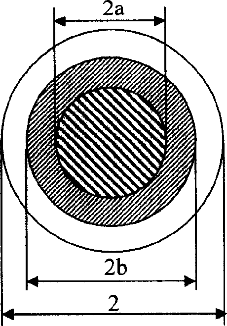
  • Figure 1
    Figure 1
  • Figure 2
    Figure 2
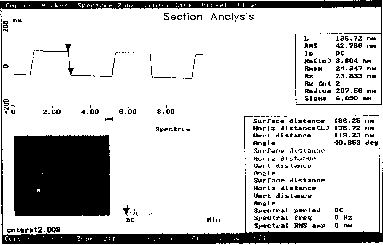
  • Figure 3
    Figure 3
Patent Text Reader

Abstract

The invention is a kind of sizing ring light beam differential confocal sensor with high spatial resolution. It includes laser device, beam expanding device, pin hole, ring light sizing device, adjustable light conjunction, polarized beam splitter, 1 / 4 wave piece, tracing inductance sensor, measuring lens, the beam splitter, collecting mirror, pin hole and two photoelectric detector behind the two holes. The invention combines the optical hyper resolution and differential confocal micro trancing technology, in order to enhance the resolution and the range of the sensor; it caters the demands of high spatial resolution, high accuracy, and large measuring range. Especially applies to the measurement of tiny structure, micro stage, tiny grooves, line width and the surface shape.
Need to check novelty before this filing date? Find Prior Art

Description

Technical field:

[0001] The invention belongs to the technical field of microscopic measurement, and in particular relates to a high spatial resolution shaped annular beam type measuring surface three-dimensional microstructure, microsteps, microstructure grooves, integrated circuit line width and surface topography by optical means. Differential confocal sensor. Background technique:

[0002] With the development of semiconductor technology to VLSI, millimeter wave and quantum devices, microfabrication technology has entered the field of deep submicron and nanometer three-dimensional processing technology. Therefore, it is very necessary to study imaging and detection technologies with large-scale and high spatial (ie vertical and horizontal) resolution capabilities that meet the requirements of this development.

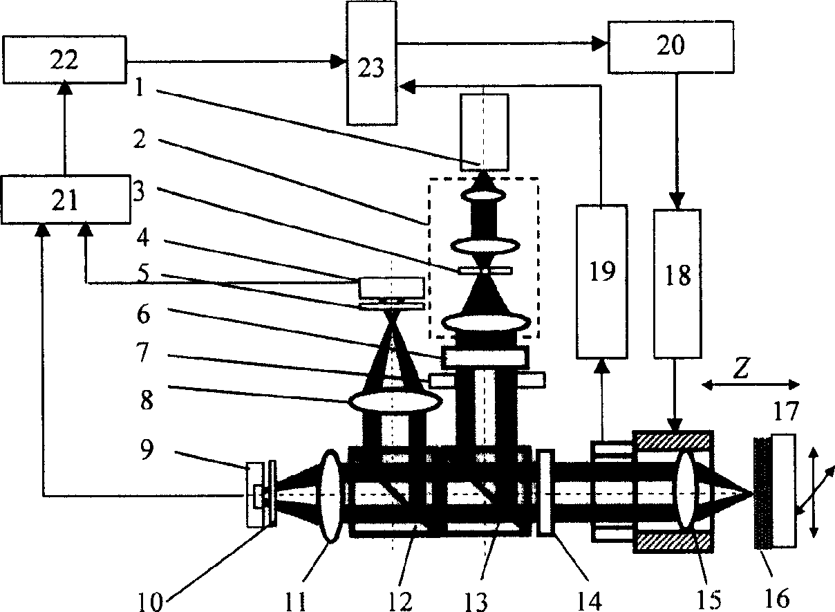
[0003] Due to the rapid development of scanning probe sensor technology based on the principles of scanning tunneling, atomic force, and near-field optics, the ...

Examples

Embodiment Construction

[0028] The structure and working principle of the high spatial resolution shaping annular beam differential confocal sensor of the present invention will be described in detail below in conjunction with the embodiments and accompanying drawings:

[0029] The structure of the high spatial resolution shaping annular beam differential confocal sensor in this embodiment is as follows figure 2 As shown, it includes: a laser 1, a beam expander 2 sequentially placed at the emitting end of the laser, a spatial filtering pinhole 3, a binary optical device 6 with circular phase distribution, and an adjustable diaphragm for adjusting the normalized radius of the incident ring light 7. Polarization beam splitter 13, a quarter wave plate 14 placed on the transmission light path of the polarization beam splitter, microscopic objective lens Z direction displacement tracking sensor 19, microscopic objective lens 15, microscopic objective lens Z direction micro displacement drive system 18, P...