

Method for preparaing Al epitaxial layer contained semiconductor material grown on GaAs substrate
An epitaxial layer and semiconductor technology, used in semiconductor lasers, semiconductor/solid-state device manufacturing, laser parts and other directions, can solve problems such as increasing materials, increasing device costs, and weakening material concentrations, and achieves increased migration length, reduced severity, Defect reduction effect
- Summary
- Abstract
- Description
- Claims
- Application Information
AI Technical Summary
Problems solved by technology
Method used
Image

Examples
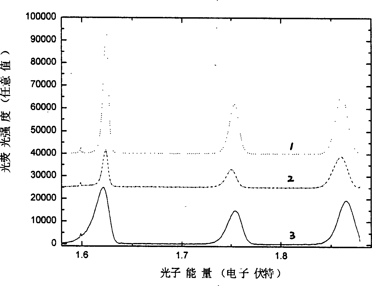
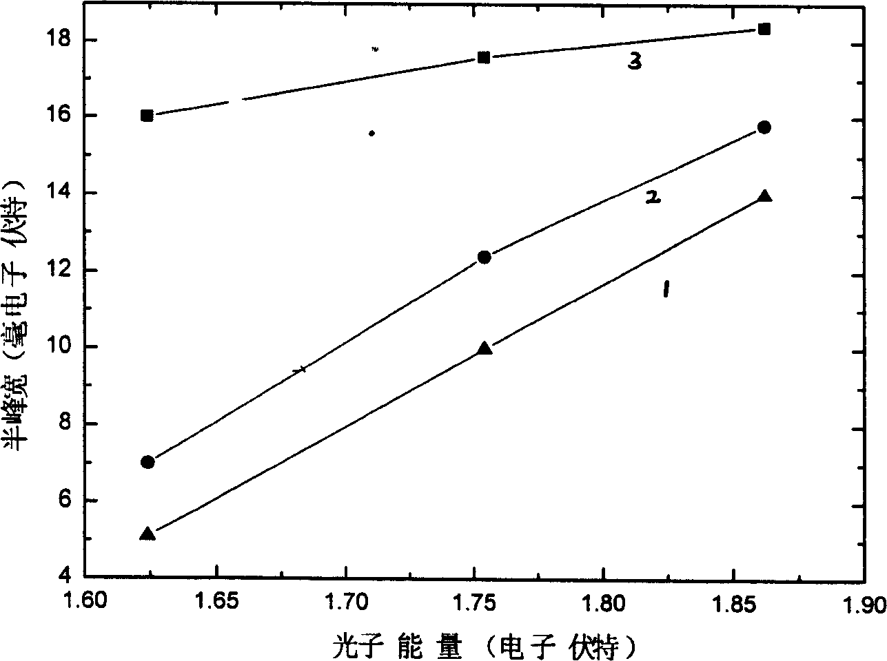
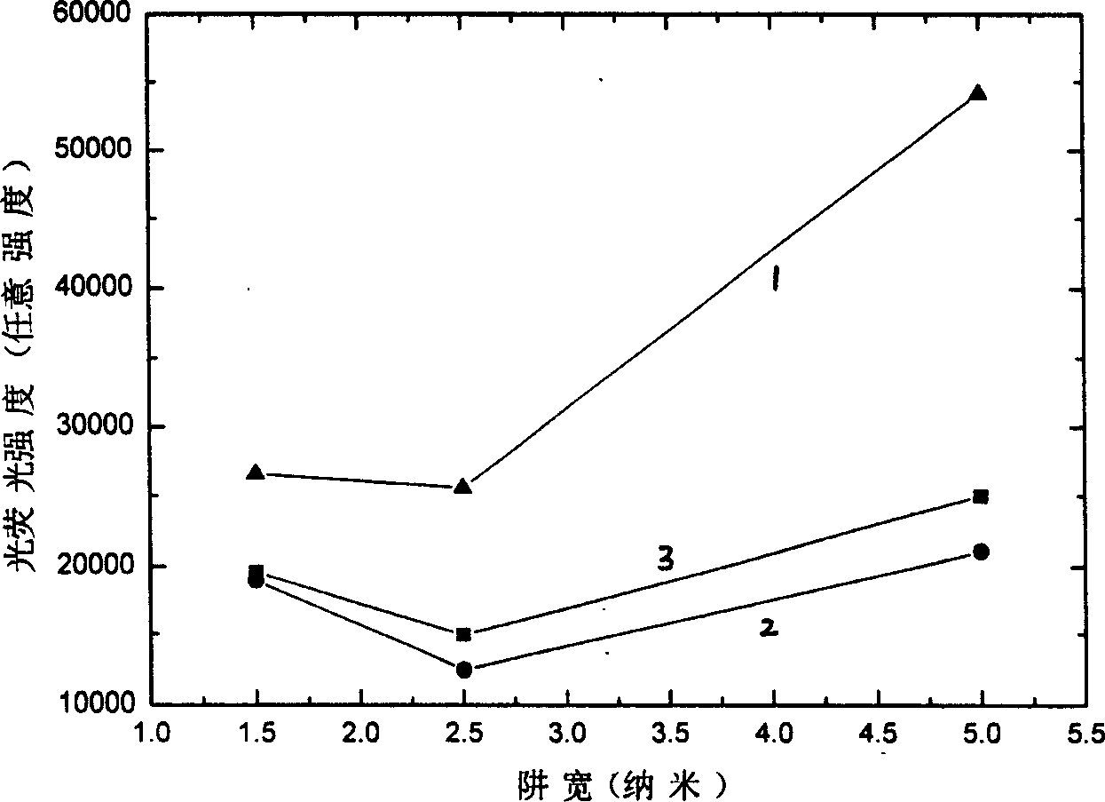
Embodiment 1
[0017] Embodiment 1: grow Al with conventional method 0.4 Ga 0.6 As / GaAs triple quantum well material
[0018] GaAs substrate at 1×10 -10 Under the background vacuum of Torr, the surface was heated to 580°C under the protection of As molecular beam to remove the surface oxide film, and then the GaAs growth rate was 500nm / hour, the Ga:As beam current ratio was 1:30, and the substrate temperature was 580°C. A 500nm thick GaAs buffer layer was grown at ℃.
[0019] At 610°C, with the above-mentioned As molecular beam, on the surface of the GaAs buffer layer with a GaAs growth rate of 500nm / hour, 833nm / hour of Al 0.4 Ga 0.6 As growth rate sequentially grows 100nm thick Al 0.4 Ga 0.6 As, 5nm thick GaAs, 50nm thick Al 0.4 Ga 0.6 As, 2.5nm thick GaAs, 50nm thick Al 0.4 Ga 0.6 As, 1.5nm thick GaAs, 100nm thick Al 0.4 Ga 0.6 As, finally covered with 3nm thick GaAs to prevent Al 0.4 Ga 0.6 The oxidation of As does not change the growth temperature and the flux of As atoms i...
Embodiment 2
[0020] Example 2: Growth of Al by interruption method 0.4 Ga 0.6 As / GaAs triple quantum well material
[0021] GaAs substrate at 1×10 -10 Under the background vacuum of Torr, the surface was heated to 580°C under the protection of As molecular beam to remove the surface oxide film, and then the GaAs growth rate was 500nm / hour, the Ga:As beam current ratio was 1:30, and the substrate temperature was 580°C. A 500nm thick GaAs buffer layer was grown at ℃.
[0022] At 610°C, with the above-mentioned As molecular beam, on the surface of the GaAs buffer layer with a GaAs growth rate of 500nm / hour, 833nm / hour of Al 0.4 Ga 0.6 As growth rate sequentially grows 100nm thick Al 0.4 Ga 0.6 As, interrupt for 30 seconds, re-grow 5nm thick GaAs, 50nm thick Al 0.4 Ga 0.6 As, stop for another 30 seconds, and then grow 2.5nm thick GaAs, 50nm thick Al 0.4 Ga 0.6 As, stop for another 30 seconds, and then grow 1.5nm thick GaAs, 100nm thick Al 0.4 Ga 0.6 As, finally covered with 3nm thi...
Embodiment 3
[0023] Example 3: growing Al-containing epitaxial layer on GaAs substrate by the method of the present invention to prepare semiconductor material by doping 1% In atom as surfactant to grow Al 0.4 Ga 0.6 As / GaAs triple quantum well material
[0024] GaAs substrate at 1×10 -10 Under the background vacuum of Torr, the surface was heated to 580°C under the protection of As molecular beam to remove the surface oxide film, and then the GaAs growth rate was 500nm / hour, the Ga:As beam current ratio was 1:30, and the substrate temperature was 580°C. A 500nm thick GaAs buffer layer was grown at ℃.
[0025] At 610°C, using the above-mentioned As molecular beam, and adding 1% In atoms to the molar number of As atoms as a surfactant, on the surface of the GaAs buffer layer, the GaAs growth rate is 500nm / hour, and the Al concentration of 833nm / hour 0.4 Ga 0.6 As growth rate sequentially grows 100nm thick Al 0.4 Ga 0.6 As, 5nm thick GaAs, 50nm thick Al 0.4 Ga 0.6 As, 2.5nm thick GaA...
PUM
 Abstract
Description
Claims
Application Information