Method for forming MTJ of magnetic RAM

A random access memory, magnetic tunnel junction technology, applied in static memory, digital memory information, information storage, etc., can solve problems such as reduced productivity, discontinuous edge level difference, difficult MTJ layer, etc., to avoid corrosion, good profile , the effect of avoiding thermal damage

Inactive Publication Date: 2004-10-20
SAMSUNG ELECTRONICS CO LTD
View PDF0 Cites 10 Cited by
  • Summary
  • Abstract
  • Description
  • Claims
  • Application Information

AI Technical Summary

Problems solved by technology

[0011] Third, in the case of performing a dry etching method using chlorine gas as an etching gas to form the MTJ layer S, there is a possibility that a discontinuous edge may be generated between the upper and lower magnetic layers S3 and S1 and the insulating layer S2 after the dry etching process. step difference
Therefore, it is difficult to form an MTJ layer with a size below a micron by dry etching
[0012] Fourth, in the case of forming the MTJ layer S using a lift-off method, productivity decreases

Method used


Image

  • Method for forming MTJ of magnetic RAM
  • Method for forming MTJ of magnetic RAM
  • Method for forming MTJ of magnetic RAM

Examples


Embodiment Construction

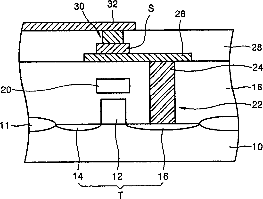
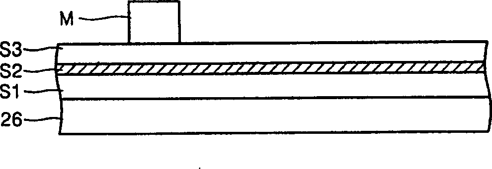
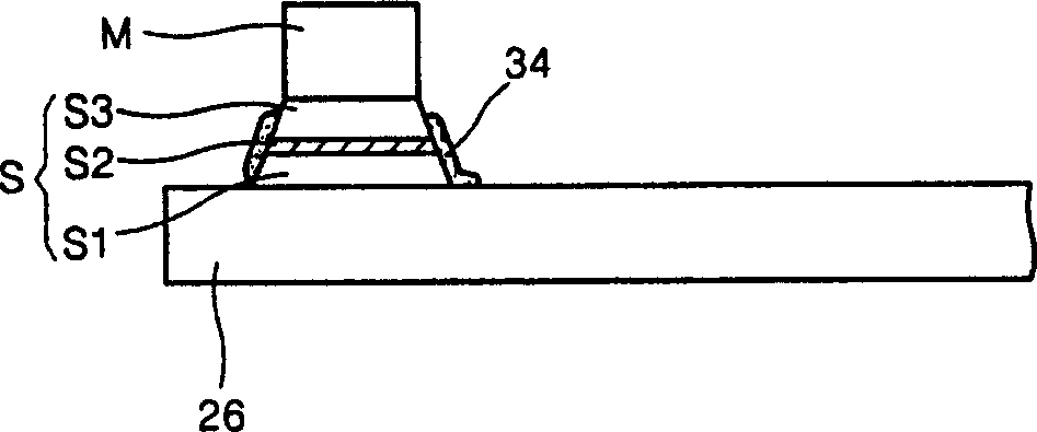
[0039] A method of forming a magnetic tunnel junction (MTJ) layer of a magnetic random access memory (MRAM) according to a preferred embodiment of the present invention will be further described below with reference to the accompanying drawings. In the drawings, the thickness of layers and regions are exaggerated for clarity.

[0040] like Figure 4 The shown method for forming the MTJ layer of the MRAM includes: forming a transistor on a substrate in step S10, and then sequentially forming a data line and an MTJ layer above the transistor by using a predetermined plasma etching process in step S20, so that the MTJ layer A transistor may be connected, and a bit line connected to the MTJ layer is formed in step S30.

[0041] refer to Figure 5 , step S10 includes: defining an active region and a field region on the substrate in step S10a, forming a field oxide layer for device insulation in the field region in step S10b, forming a gate stack including a gate in step S10c A sou...


PUM


Abstract

A method of forming a magnetic tunneling junction (MTJ) layer for an MRAM includes sequentially forming a lower material layer, an insulation layer, and an upper material layer on a substrate, forming a mask pattern on a predetermined region of the upper material layer, sequentially removing the upper material layer, the insulation layer, and the lower material layer from around the mask pattern using plasma generated from an etching gas, wherein the etching gas is a mixture of a main gas and an additive gas having a predetermined mixture ratio and including no chlorine (Cl2) gas, and removing the mask pattern. Accordingly, an MTJ layer formed by the method may incur no thermal damage due to high temperature etching, no material deposits due to by-products of etching, and no step difference or corrosion due to chlorine gas, and may have an excellent profile.

Description

technical field [0001] The present invention relates to a method of manufacturing a magnetic random access memory (MRAM), and more particularly, to a method of forming a magnetic tunnel junction (MTJ) of the MRAM. Background technique [0002] like figure 1 As shown, the MRAM generally includes a transistor T used as a switch and an MTJ layer S, where data with a value of "0" or "1" is recorded on the MTJ layer. [0003] The following will refer to figure 1 A conventional method of fabricating MRAM is described. A gate stack 12 including a gate is formed on the semiconductor substrate 10 , and then a source region 14 and a drain region 16 are respectively formed on both sides of the gate stack 12 , thereby forming a transistor T with a switching function. exist figure 1 , reference numeral 11 represents a field oxide layer. An interlayer dielectric layer 18 is formed on the semiconductor substrate 10 on which the transistor T has been formed so as to completely cover th...

Claims


Application Information

Patent Timeline
Patent Type & Authority Applications(China)
IPC IPC(8): H01L21/3065G11C11/14G11C11/15G11C11/16H01L21/302H01L21/336H01L21/461H01L21/70H01L21/8246H01L27/105H01L27/22H01L43/12
CPCG11C11/16B82Y10/00H01L43/12H01L27/228H10B61/22H10N50/01G11C11/15
Inventor 黄淳元宋利宪金泰完
Owner SAMSUNG ELECTRONICS CO LTD
Why Eureka
Try Eureka