Super resolution reflecting film arrangement
A super-resolution and reflective film technology, applied in the field of optical storage, to achieve the effect of simple film structure, simple process, and low production cost
- Summary
- Abstract
- Description
- Claims
- Application Information
AI Technical Summary
Problems solved by technology
Method used
Image
Examples
Embodiment Construction
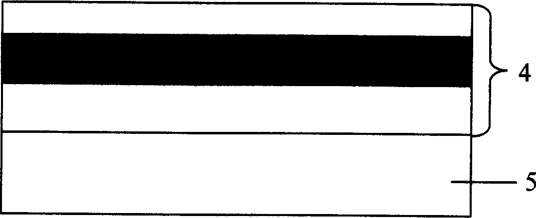
[0018] The structure of the super-resolution reflective film of the present invention is as follows figure 1 As shown, a protective layer 1, a super-resolution reflective film 2 and a protective layer 3 are included. The protective layer 1 and the protective layer 3 are used to prevent the super-resolution reflective film 2 from being damaged or oxidized, and the super-resolution reflective film 2 is used to read out the super-resolution information recording point.
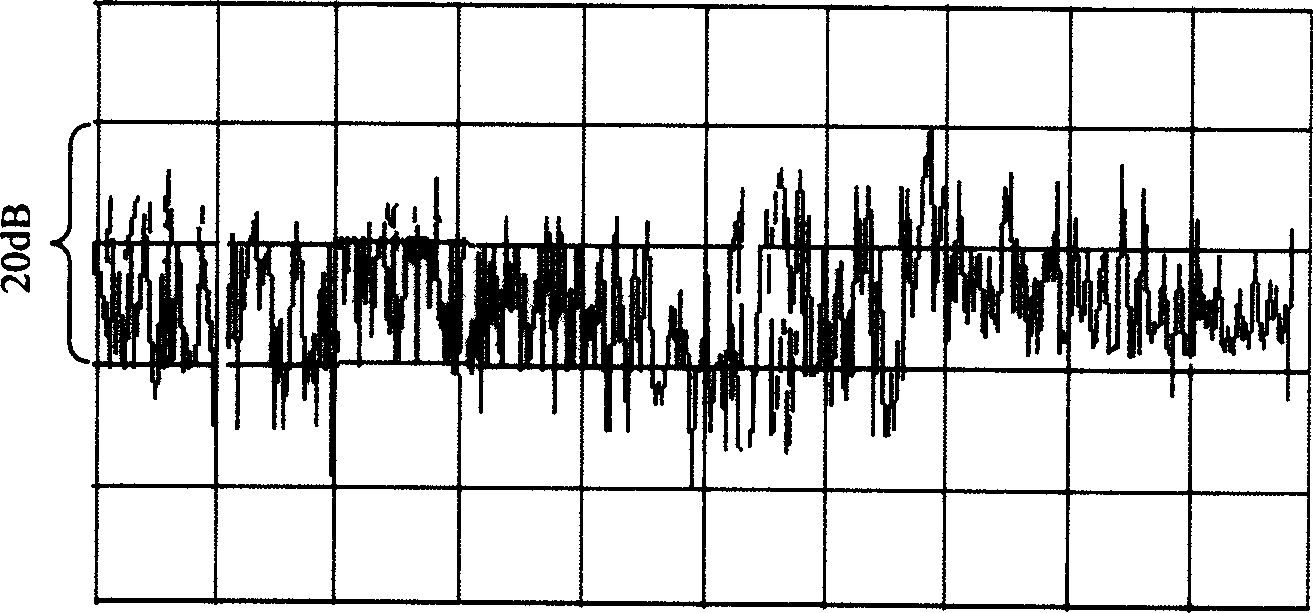
[0019] The protective layer 1 and the protective layer 3 in the present invention are both composed of silicon nitride with a thickness of 50-100 nm, and the super-resolution reflective film 2 is composed of antimony (Sb) or silicon (Si) or titanium (Ti) with a thickness of 5-50 nm , Take the value according to the specific situation of the implementation. The protective layer 1, the super-resolution reflective film 2 and the protective layer 3 jointly form the super-resolution reflective film structure 4, see figur...
PUM
| Property | Measurement | Unit |
|---|---|---|
| thickness | aaaaa | aaaaa |
| thickness | aaaaa | aaaaa |
| diameter | aaaaa | aaaaa |
Abstract
Description
Claims
Application Information


