Method for making device with transistors of different types

A type of transistor and type of technology, applied in the direction of transistors, semiconductor devices, electric solid state devices, etc., to achieve the effects of improving performance, high electron mobility, and reducing costs

Inactive Publication Date: 2004-12-01
IBM CORP +1
View PDF0 Cites 2 Cited by
  • Summary
  • Abstract
  • Description
  • Claims
  • Application Information

AI Technical Summary

Problems solved by technology

However, apart from the extra effort involved in such chemical treatments, they only allow a limited range of possible material changes without adversely affecting other parts of the device.
In addition, some conventional techniques employ organic thin film deposition methods; however, these methods often suffer from compatibility issues with subsequent thermal treatments
In addition, some conventional processes require separate growth of gate oxides for different types of transistors, and also require independent patterning of different types of gate conductors

Method used


Image

  • Method for making device with transistors of different types
  • Method for making device with transistors of different types
  • Method for making device with transistors of different types

Examples


Embodiment Construction

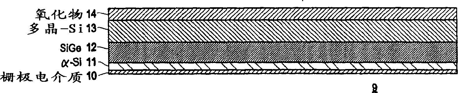
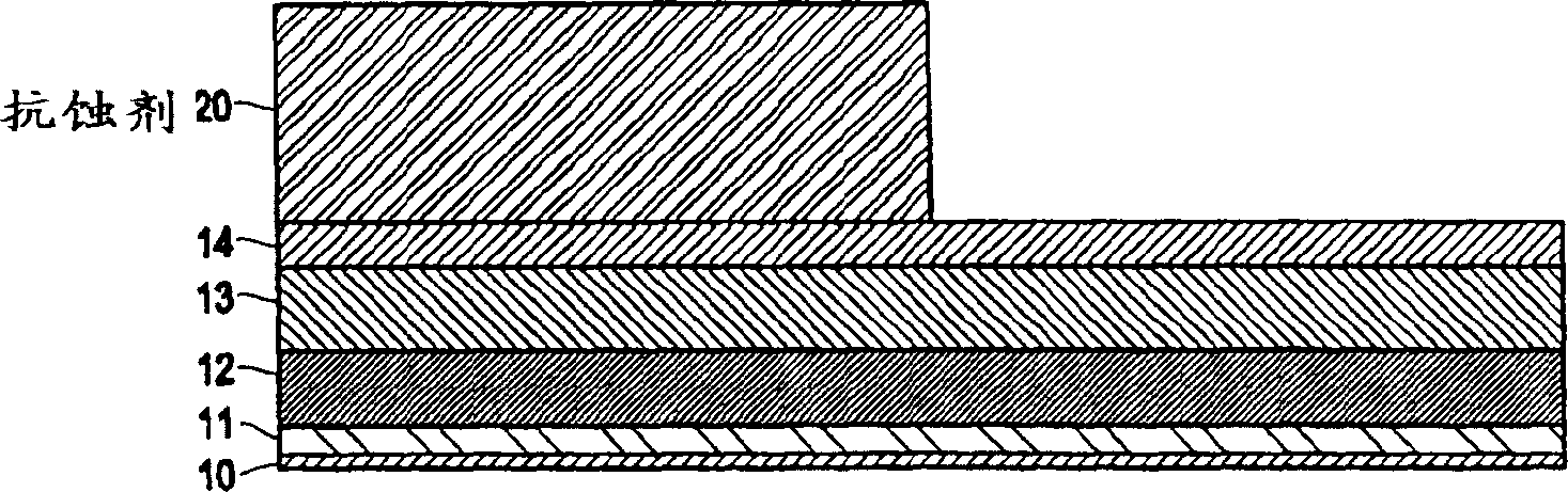
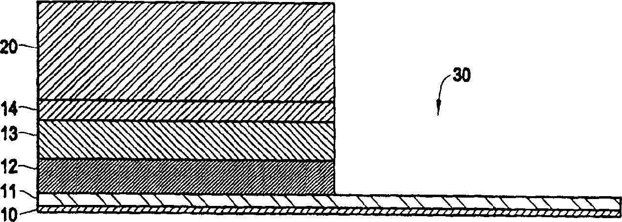
[0023] As described above, the present invention provides a process in which gate oxides can be formed simultaneously for all transistors of different materials and in which all gate conductors of the transistors can be patterned simultaneously. this is in Figure 1-10 The schematic partial cross-sectional view of the integrated circuit shown is shown in greater detail. More specifically, figure 1 Illustrates the upper portion of the base substrate 9 when growing a gate dielectric, which may be an oxide, oxynitride, or a high-k dielectric (any compatible type), on the base substrate 9, which may be bulk silicon or silicon-on-insulator The gate dielectric 10 formed in . An amorphous silicon layer 11 , a silicon germanium layer 12 and a polysilicon layer 13 are then sequentially deposited on the gate dielectric 10 . The present invention can deposit these layers using any conventional deposition process such as any form of chemical vapor deposition (CVD) or physical vapor dep...


PUM


Abstract

A method and structure for a method of manufacturing a device having different types of transistors, wherein gates of the different types of transistors in the device comprise different materials. The method comprises depositing a silicon layer on a gate dielectric layer, depositing a first-type gate material on the silicon layer, removing the first-type gate material from areas where a second-type gate is to be formed, depositing a second-type gate material on the silicon layer in areas where the first-type gate material was removed, and simultaneously patterning the first-type gate material and the second-type gate material into first-type and second-type gates, and anneal and transform the two types of gate materials.

Description

technical field [0001] The present invention generally relates to methods of fabricating devices employing different types of transistors, and more particularly to forming all gate oxides in a single step and simultaneously patterning all gate conductors with different materials in a single step craft. Background technique [0002] Recent advances in integrated circuit chip fabrication processes have allowed the simultaneous fabrication of different types of transistors (N-type and P-type) on a single chip, each type of gate electrode formed from a different material. This allows the performance of integrated circuit chips to be improved without increasing the manufacturing cost or time required to manufacture the chips. [0003] However, the process for fabricating integrated circuit chips of various transistors using various gate conductor materials can still be further streamlined. For example, many common techniques perform redundant processing whereby different previo...

Claims


Application Information

Patent Timeline
Patent Type & Authority Applications(China)
IPC IPC(8): H01L21/28H01L21/336H01L21/8238H01L27/08H01L27/092H01L29/423H01L29/49H01L29/786
CPCH01L21/823842
Inventor 陈佳安德里亚斯·E·格拉斯曼
Owner IBM CORP
Why Eureka
Try Eureka