Method for fabricating a nanoarray using the self-assembly of supramolecules and staining of metals
A supramolecular, self-assembly technology, applied in chemical instruments and methods, biochemical equipment and methods, nanotechnology, etc., can solve the problems of complex thin film structure, failure to develop diagnostic protein nanochips, and complex processes
- Summary
- Abstract
- Description
- Claims
- Application Information
AI Technical Summary
Problems solved by technology
Method used
Image


Examples
preparation example Construction
[0063] The preparation method of the DNA chip in the biological chip of the present invention includes the step of connecting the pre-prepared probes to the surface of the solid substrate by means of a spotting method. In this case, the amine-bound probe is dissolved in 1X to 7X, preferably 2X to 5X, more preferably 3X SSC buffer solution (0.45M NaCl, 15mM C 6 h 5 Na 3 o 7 , pH 7.0), and then use a microarray spotter to spot it onto the substrate with aldehyde groups attached. Then, the probes are immobilized on the substrate by utilizing the interaction between aldehyde groups and amine groups. The concentration of probe used is greater than 10 pmol / μl, preferably greater than 50 pmol / μl, more preferably greater than 100 pmol / μl. The amine group combined with the probe and the aldehyde group combined with the substrate react with each other for 4-8 hours, preferably 5-7 hours, most preferably about 6 hours under the condition of 70-90%, preferably 80%, in humidity, so tha...
Embodiment 1
[0067] Embodiment 1: the synthesis of supramolecular
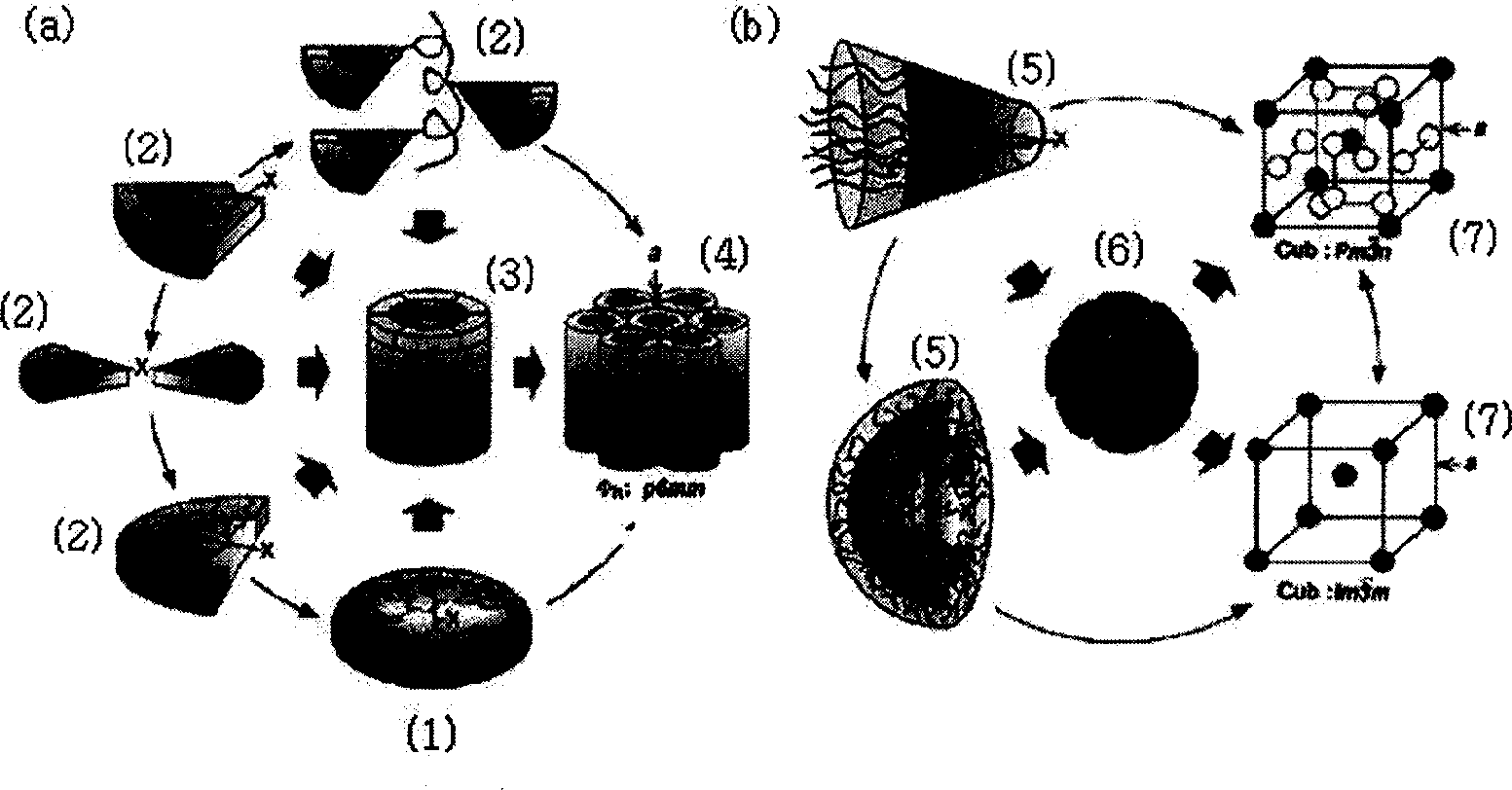
[0068] The supramolecule of formula (1) used in the present invention is synthesized through the steps of the following reaction scheme (1). The scanning electron microscope analysis of the supramolecule confirmed that the supramolecule is a regular cylindrical structure of nanoscale or smaller scale.
[0069] (Reaction Diagram 1)
[0070]
Embodiment 2
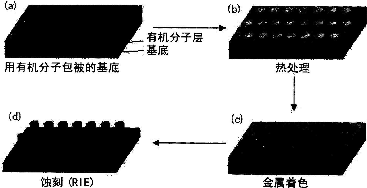
[0071] Embodiment 2: substrate surface modification
[0072] In the present invention, a silicon wafer is used as a substrate. Metallic, non-metallic, or other thin films may be formed on the surface of the substrate, if desired.
PUM
 Abstract
Description
Claims
Application Information