Organic field effect transistor orientation layer and its preparing method and use

An orientation layer, organic field technology, applied in semiconductor/solid-state device manufacturing, electrical components, electrical solid-state devices, etc., can solve problems such as breakdown of OFETs, surface unevenness of rayon, and effects of OFET switching characteristics

Inactive Publication Date: 2005-03-02
FUDAN UNIV
View PDF0 Cites 6 Cited by
  • Summary
  • Abstract
  • Description
  • Claims
  • Application Information

AI Technical Summary

Problems solved by technology

However, a large amount of dust and charged particles generated during the rubbing process may adhere to the orientation layer, causing pollution and increasing the defect density of the orientation layer; moreover, surface irregularities such as rayon and nylon may cause orientation Inhomogeneity; Moreover, the electrostatic charge generated during the friction process will also affect the switching characteristics of the OFET, and if it is serious, it may break down the channel of the OFET and destroy the OFET device

Method used


Image

  • Organic field effect transistor orientation layer and its preparing method and use
  • Organic field effect transistor orientation layer and its preparing method and use
  • Organic field effect transistor orientation layer and its preparing method and use

Examples


Embodiment

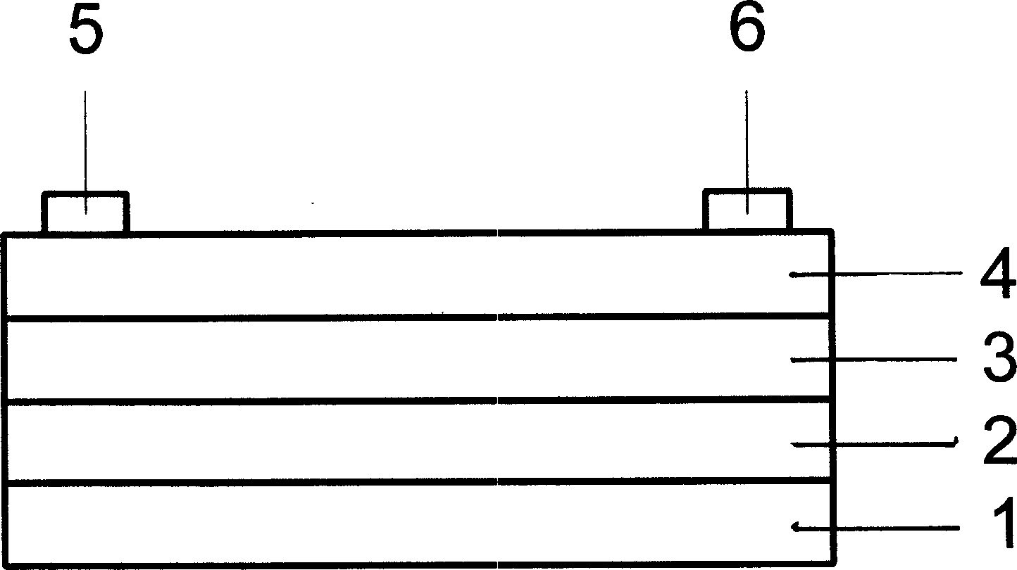
[0037] The polyimide (PI) we used was RN-1333 type PI provided by Nissan Chemical Industry at a concentration of 5 wt%. We dilute it to 2wt% when using it. First form an ITO electrode on a clean glass substrate, and then use photolithography to form a gate pattern on the substrate. After the polyimide (PI) solution is dispersed by ultrasonic waves for 20-30 minutes, it is spin-coated on On the ITO glass substrate, control a certain spin-coating speed and time. Then place the coated substrate on a hot table at 100°C to dry for 5 minutes for pre-baking treatment, and then place it in a clean oven at 250°C for 1 hour to perform film hardening treatment. Thereafter, it was naturally cooled to room temperature.

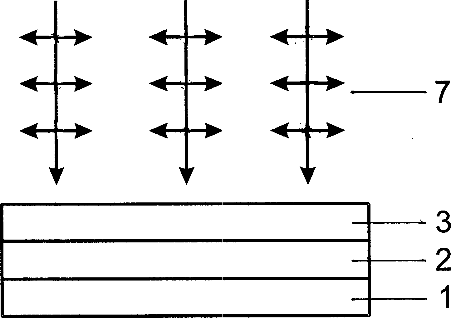
[0038] Then, with a power density of 10mW / cm 2 The ultra-high pressure mercury lamp directly irradiates linearly polarized ultraviolet light with a spectral peak of about 365nm onto the above-mentioned orientation insulating layer vertically, as shown in the attached ...


PUM


Abstract

The invention provides an orientation layer used for organic field-effect transistor, a method for forming the orientation layer and a new component using said orientation layer as insulating layer to increase carrier mobility of organic field-effect transistor. The orientation layer is composed of polyimide (PI) type polymer by optical orientation processing. BY the invention, good orientation effect on PI orientation layer is obtained, carrier mobility of organic semiconductor transmission layer is increased, order degree of molecule arranging on organic semiconductor transmission layer is improved, thus channel carrier mobility characteristic of organic field-effect transistor (OFET) using said orientation layer as insulating layer is improved largely.

Description

technical field [0001] The invention belongs to the technical field of organic field-effect transistors (OFETs), and in particular relates to an orientation layer with excellent orientation characteristics, a preparation method and application thereof. technical background [0002] Field Effect Transistor (FET) uses the gate voltage to control the on-off of the channel current to form the required switching characteristics. An organic field effect transistor (OFET) or an organic thin film transistor (OTFT) uses an organic semiconductor polymer as an insulating layer and an organic semiconductor transport layer, and the principle is the same as that of an ordinary field effect transistor. Compared with inorganic electronic devices, the preparation method of organic electronic devices is simple, low in cost, suitable for making large-area devices, and can also be prepared on polymer substrates to obtain flexible devices. Therefore, it has very broad application prospects. Fro...

Claims


Application Information

Patent Timeline
Patent Type & Authority Applications(China)
IPC IPC(8): H01L51/30H01L51/40
Inventor 许军李岩川黄维
Owner FUDAN UNIV
Why Eureka
Try Eureka