High-speed three-dimension integrated circuit active layer structure and manufacturing method

A technology of integrated circuits and active layers, applied in circuits, electrical components, electric solid-state devices, etc., can solve the problem of low speed of three-dimensional integrated circuits, and achieve the effect of ensuring AC and DC electrical performance and avoiding influence

Inactive Publication Date: 2005-03-23
XIDIAN UNIV
View PDF0 Cites 2 Cited by
  • Summary
  • Abstract
  • Description
  • Claims
  • Application Information

AI Technical Summary

Problems solved by technology

[0014] One of the purposes of the present invention is to provide a high-speed three-dimensional integrated circuit active layer structure, and the second object is to provide a method for making this active layer structure to solve the problem of the low speed of the existing three-dimensional integrated circuit made of Si material. The problem

Method used


Image

  • High-speed three-dimension integrated circuit active layer structure and manufacturing method
  • High-speed three-dimension integrated circuit active layer structure and manufacturing method
  • High-speed three-dimension integrated circuit active layer structure and manufacturing method

Examples


Embodiment 1

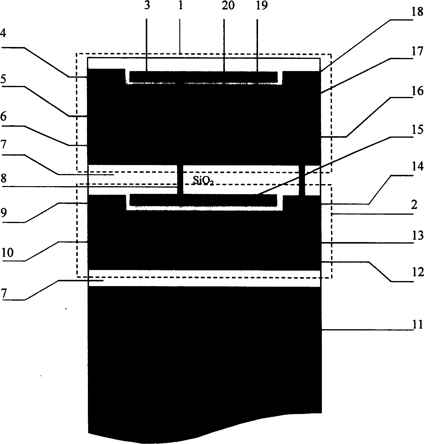
[0038] like figure 1 As shown, in the first embodiment of this description, the active layer of the CMOS IC is composed of the SiGe / Si SOI quantum well active layer and the SiSOI active layer. The structure has upper and lower layers, of which 1 is SiGe / Si pMOS field effect transistor; 2 is Si nMOS field effect transistor; 3 is pMOS field effect transistor Ploy-Si gate; 4 is pMOS Ploy-Si source; 5 is pMOS Source region; 6 is pMOS substrate region; 7 is insulating layer; 8 is Ploy-Si interconnection line; 9 is nMOS Ploy-Si source; 10 is nMOS source region; 11 is substrate; 12 is nMOS drain region; 13 is the nMOS channel substrate region; 14 is the nMOS Ploy-Si drain; 15 is the nMOS field effect transistor Ploy-Si gate; 16 is the Ploy-Si interconnection line; 17 is the pMOS drain region; 18 is the pMOS drain ; 19 is the MOS channel region; 20 is the cap layer.

[0039] The pMOS gate 3 , source 4 , source region 5 , substrate region 6 , insulating layer 7 , drain region 17 , dr...

Embodiment 2

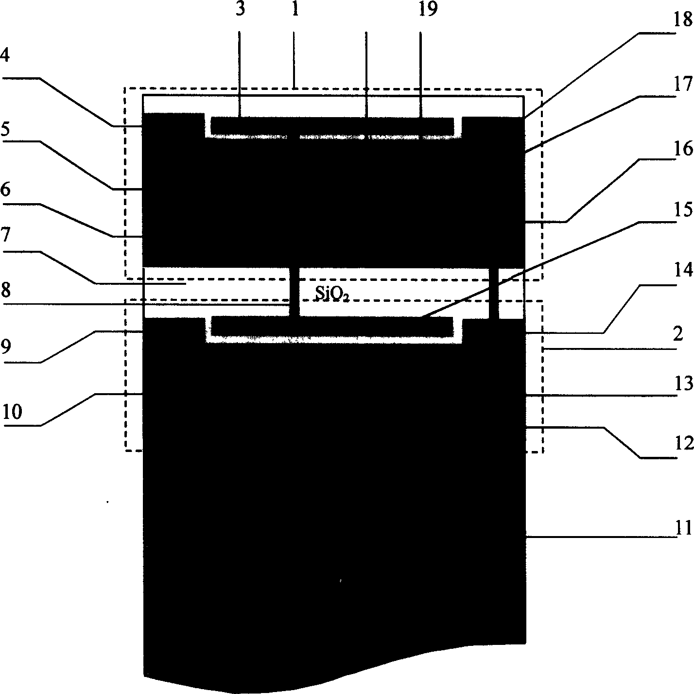
[0043] like figure 2 As shown, the second embodiment of this description is a structure in which the active layer of the CMOS IC is formed by the SiGe / Si SOI surface channel active layer and the Si SOI active layer. The structure has upper and lower layers, of which 1 is SiGe / Si pMOS field effect transistor; 2 is Si nMOS field effect transistor; 3 is pMOS field effect transistor Ploy-Si gate; 4 is pMOS Ploy-Si source; 5 is pMOS Source region; 6 is pMOS substrate region; 7 is insulating layer; 8 is Ploy-Si interconnection line; 9 is nMOS Ploy-Si source; 10 is nMOS source region; 11 is substrate; 12 is nMOS drain region; 13 is the nMOS channel substrate region; 14 is the nMOS Ploy-Si drain; 15 is the nMOS field effect transistor Ploy-Si gate; 16 is the Ploy-Si interconnection line; 17 is the pMOS drain region; 18 is the pMOS drain ; 19 is the MOS channel region.

[0044] The pMOS gate 3 , source 4 , source region 5 , substrate region 6 , insulating layer 7 , drain region 17 a...

Embodiment 3

[0048] like image 3 As shown, in the third embodiment of this description, the active layer of the CMOS IC is composed of the SiGe / Si SOI quantum well channel active layer and the Si active layer. The structure has two layers, 1 is SiGe / SipMOS field effect transistor; 2 is Si nMOS field effect transistor; 3 is pMOS field effect transistor Ploy-Si gate; 4 is pMOS Poly-Si source; 5 is pMOS source 6 is the pMOS substrate area; 7 is the insulating layer; 8 is the Ploy-Si interconnection line; 9 is the nMOS Ploy-Si source; 10 is the nMOS source area; 11 is the substrate; 12 is the nMOS drain area; 13 14 is nMOS Ploy-Si drain; 15 is nMOS field effect transistor Ploy-Si gate; 16 is Ploy-Si interconnection; 17 is pMOS drain; 18 is pMOS drain; 19 is a MOS channel region; 20 is a cap layer.

[0049] The pMOS gate 3 , source 4 , source region 5 , substrate region 6 , insulating layer 7 , drain region 17 , drain 18 , channel region 19 and cap layer 20 constitute a pMOS field effect tra...


PUM


Abstract

The invention discloses an active structure of the high speed three dimensional integrated circuits and its preparation method and aims to increase the speed of today's three dimensional integrated circuits. The invention adopts the single crystal of Si and SiGe / Si to build the two active layers of the new three dimensional integrated circuits. The first active layer chooses the Si SOI or substrate of Si to produce the n-type channel MOS field effect transistor nMOS. The second active layer chooses the substrate of SiGe / Si SOI to produce the p-type channel MOS field effect transistor pMOS. We adopt the low temperature technique to realize the bonding between the two layers and prepare the second active material and device as at low temperature to avoid the effect of the high temperature to the structure of the preliminary active device and to guarantee the alternating current-direct current electric property of the three dimensional integrated circuits. The active structure of he invention can be used in producing the three dimensional CMOS integrated circuits as well as the BiCMOS integrated circuits. Based on the feature of high cavity mobility of SiGe / Sip MOS field effect transistor, compared with today's three dimensional integrated circuits, the three dimensional integrated circuits produced through the active layer of the invention is featured by the high speed and good property.

Description

technical field [0001] The invention belongs to the technical field of semiconductor integrated circuits, and in particular relates to a structure and a manufacturing method of an active layer of a high-speed three-dimensional integrated circuit. Background technique [0002] Integrated circuits follow Moore's (Note: Moore's name) law, and the feature size continues to decrease, and the integration and performance of chips continue to improve. Entering the deep submicron era, the interconnection of devices inside the chip has become more and more complex, and the area occupied by the interconnection line is almost equal to the area of ​​the device. Therefore, the influence of the delay time caused by the parasitic resistance and parasitic capacitance of the interconnection on the performance of the circuit becomes more and more prominent. Studies have shown that after the feature size of the device is less than 250nm, the R-C delay caused by conventional metal wiring will d...

Claims


Application Information

Patent Timeline
Patent Type & Authority Applications(China)
IPC IPC(8): H01L21/82H01L21/8238H01L21/84H01L27/092H01L27/12
Inventor 张鹤鸣胡辉勇戴显英舒斌王喜媛朱国良王伟姜涛朱勇刚
Owner XIDIAN UNIV
Why Eureka
Try Eureka