

Process for controlling denuded zone depth in an ideal oxygen precipitating silicon wafer
A technology of oxygen precipitation and silicon wafers, which is applied in semiconductor/solid-state device manufacturing, electrical components, circuits, etc., and can solve the problems of high interstitial oxygen concentration and reducing the resistivity of silicon wafer device layers.
- Summary
- Abstract
- Description
- Claims
- Application Information
AI Technical Summary
Problems solved by technology
Method used
Image

Examples
example 1
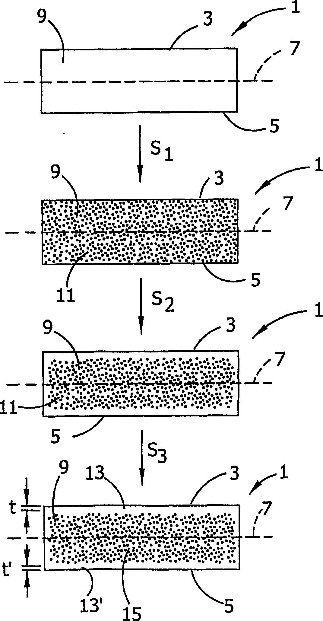
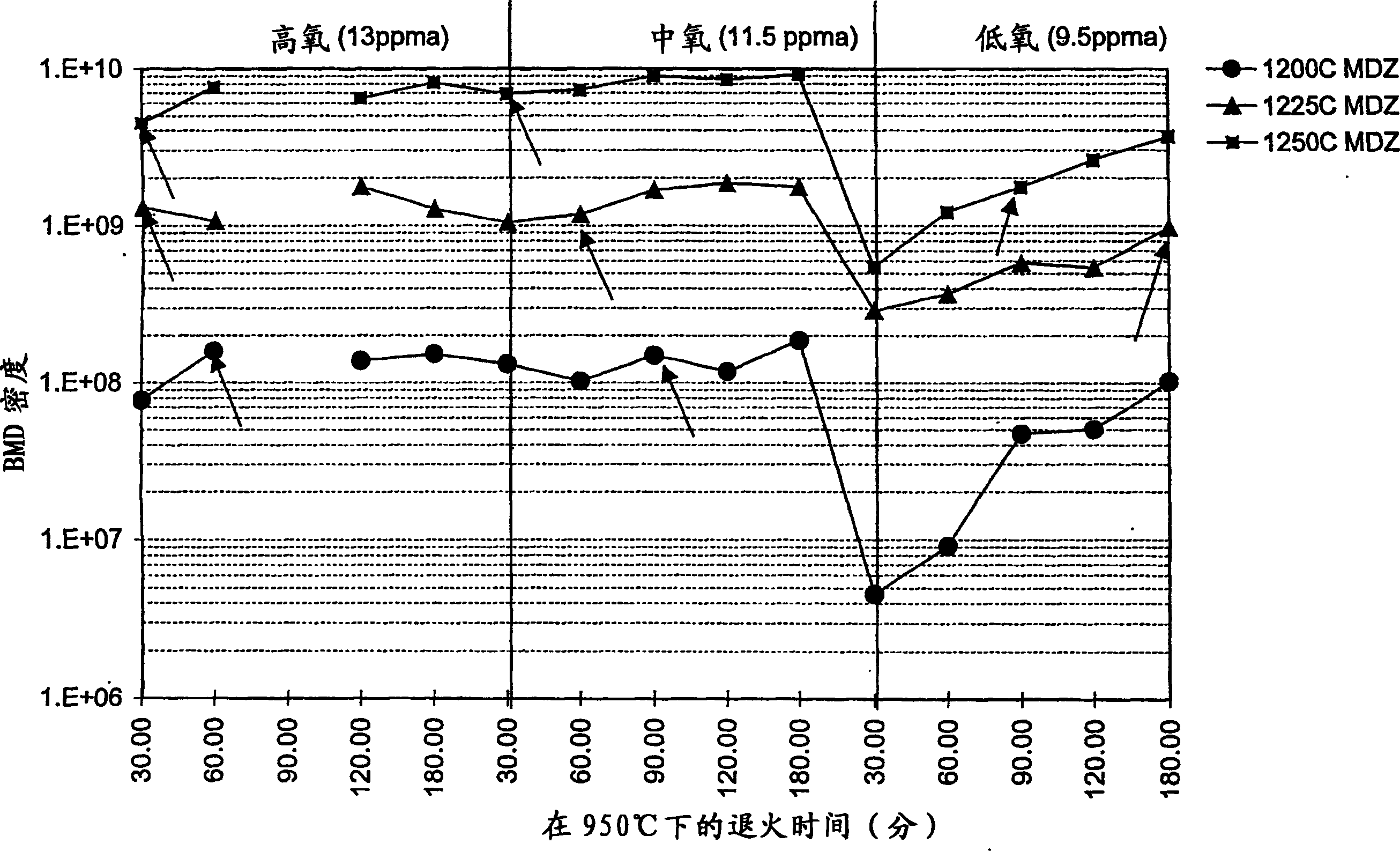
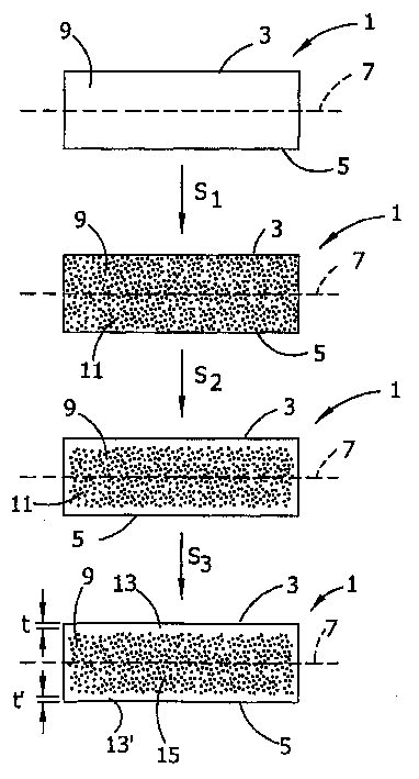
[0071] Example 1 and figure 2 Indicates the gettering capacity of an ideal deposited silicon wafer in a range of oxygen concentrations. In the first set of experiments, an ideal precipitated silicon wafer with an oxygen concentration of 13PPMA was heat-treated at 1200°C in step S 1 Formation followed by bulk precipitation of oxygen grows at a temperature of 950° C. in the range of 30-180 minutes. Repeat step S with heat treatment temperature of 1225°C and 1250°C 1 . In the second and third sets of experiments, the first set of experiments was repeated on ideal precipitated silicon wafers with 11.5 PPMA and 9.5 PPMA oxygen precipitation concentrations, respectively. The gettering ability was measured by contaminating the rear surface of the silicon wafer with nickel. figure 2 The arrow in indicates the start of complete aspiration. The data show that for ideally precipitated silicon wafers over a range of oxygen concentrations, even at low oxygen concentrations, bulk dep...
example 2
[0073] Four silicon wafers were cut from two segments of high-resistivity CZ crystal. Three silicon wafers were ideally heat-treated for precipitated silicon wafers at 1235°C, 1250°C and 1275°C respectively. The fourth wafer is a controller, without ideal thermal treatment of precipitated wafers. Each wafer was then quartered and subjected to the following secondary annealing:
[0074] Wafer GG, quarter 1 (GGQ1): 4 hours at 800°C, followed by 16 hours at 1000°C;
[0075] Wafer GG, quarter 2 (GGQ2): 8 hours at 800°C, followed by 16 hours at 1000°C;
[0076] Wafer GG, quarter 3 (GGQ3): ramp from 800°C to 1000°C at a rate of 1°C / min, followed by 1 hour at 1000°C; and
[0077] Wafer GG, quarter 4 (GGQ4): Ramp from 800°C to 1000°C at a rate of 2°C / min, followed by 1 hour at 1000°C.
[0078] silicon wafer
[0079] The control wafers did not receive ideal precipitated wafer processing, so the precipitate density after thermal cycles was derived from pre-existing precipita...
example 3
[0081] silicon wafer
[0082] The 800°C-1000°C ramp anneal (Q3 and Q4) is not very effective at growing the precipitates formed during the ideal precipitated wafer process, thereby removing little interstitial oxygen in solution. In contrast, the two-step 800°C and 1000°C anneals (Q1 and Q2) were much more effective at growing the precipitates formed during the ideal precipitated wafer process and removing interstitial oxygen in solution. Additionally, the 8 hr / 800°C anneal is more effective at removing interstitial oxygen than the 4 hr / 800°C anneal. Moreover, the final O after the two-step annealing i It decreases with the increase of the high temperature annealing temperature of the ideal precipitated silicon wafer. Finally, the data show that the final O i With initial O i Varies, the higher the initial O i This provides greater supersaturation which results in a greater removal of interstitial oxygen from solution during the secondary anneal.
PUM
 Abstract
Description
Claims
Application Information