Method for processing graphene superlattice nano-structure with atomic force microscope

An atomic force microscope and nanostructure technology, applied in the fields of nanostructure manufacturing, nanotechnology, nanotechnology, etc., can solve the problems of difficult processing, reduce the electrical properties of devices, and roughness of graphene, and achieve the effect of simple processing methods.

Inactive Publication Date: 2014-05-14
INST OF PHYSICS - CHINESE ACAD OF SCI
View PDF3 Cites 10 Cited by
  • Summary
  • Abstract
  • Description
  • Claims
  • Application Information

AI Technical Summary

Problems solved by technology

[0004] This kind of graphene superlattice nanostructure can be prepared by traditional micro-processing methods, but its processing is difficult, and the resolution is limited by the neighbor effect of electron beam exposure. It is difficult to control the period of the holes below 200nm.
The prior art provides a structure of using self-assembled copolymer nanoparticles as a mask to p...

Method used


Image

  • Method for processing graphene superlattice nano-structure with atomic force microscope

Examples


Embodiment Construction

[0022] The technical solutions of the present invention will be further described below in conjunction with the accompanying drawings and through specific implementation methods.

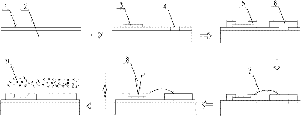
[0023] Such as figure 1 As shown, in this embodiment, the present application provides a method for processing graphene superlattice nanostructures using an atomic force microscope, which includes: Step A: using the needle tip 8 of the atomic force microscope to apply a pulse voltage to the graphene 3 artificial vacancy defects.

[0024] Step B: using hydrogen-containing plasma 9 to anisotropically etch the graphene 3 .

[0025] The method of adding pulse voltage to the tip of the atomic force microscope is used to artificially introduce periodic vacancy defects, the smallest period of which can reach 50nm, and then processed by hydrogen plasma9 to make the boundary of the cavity form an atomically smooth zigzag (serrated) boundary, At the same time, the size of graphene 3 nanoribbons can be accur...


PUM

PropertyMeasurementUnit
Diameteraaaaaaaaaa

Abstract

The invention relates to the technical field of nano processing, in particular to a method for processing a graphene superlattice nano-structure with an atomic force microscope. The method for processing the graphene superlattice nano-structure with the atomic force microscope comprises the steps that a manual vacancy defect is formed on graphene in the mode of applying pulse voltages to a needle point of the atomic force microscope, and then anisotropic etching is carried out on the graphene through a hydrogen-contained plasma. According to the method, nano hole array patterns with a period smaller than a 200 nm can be achieved on the graphene. The period of the graphene superlattice nano-structure and nanoribbon width are controllable. A processing method of the needle point of the atomic force microscope is simple and free of inducing additional pollution means, and an obtained device is clean. In addition, with the assistance of the needle point array processing technology, the method can be used for device integration and mass production of graphene nano-structure devices.

Description

technical field [0001] The invention relates to the technical field of nano-processing, in particular to a method for processing graphene superlattice nanostructures by using an atomic force microscope. Background technique [0002] Graphene is a monoatomic layer of graphite with excellent electrical properties. Its electron mobility is as high as 100,000cm2V-1s-1. It was first prepared by scientists from the University of Manchester in 2004 (Science306,666(2004)). Electrons in single-layer graphene have a linear dispersion relationship near the Dirac point, and belong to massless Dirac fermions, whose Fermi speed is 1 / 300 of the speed of light. Therefore, the discovery of this material is a study of the physical properties of condensed matter materials. And computing provides an ideal way to realize it. [0003] The electrical properties of the graphene superlattice porous nanostructure are affected by both the quantum confinement effect and the modulation of the periodic ...

Claims


Application Information

Patent Timeline
IPC IPC(8): B82B3/00B82Y40/00
Inventor 成蒙张广宇时东霞
Owner INST OF PHYSICS - CHINESE ACAD OF SCI
Why Eureka
Try Eureka