Electrophotographic photoconductor

a photoconductor and electroctrophotography technology, applied in the direction of electrographic process apparatus, instruments, corona discharge, etc., can solve the problems of electrical characteristics that cannot reach the required level, electrical characteristics suffer from deterioration of electrical characteristics, and increase of residual potential, so as to achieve stable and excellent charging characteristics

Inactive Publication Date: 2001-10-09
FUJI ELECTRIC CO LTD
View PDF2 Cites 10 Cited by
  • Summary
  • Abstract
  • Description
  • Claims
  • Application Information

AI Technical Summary

Benefits of technology

In view of the foregoing, it is an object of the present invention to provide an electrophotographic photoconductor that exhibits a stable and excellent charging characteristic and allows utilization of the first turn of the photoconductor for image formation.

Problems solved by technology

The charge transport layer of conventional photoconductors suffers from deterioration of electrical characteristics, for example increase of residual potential, due to charge trapping at the trapping sites existing in, for example, the intermediate product included as impurities of synthesis process of the charge transport material, the residue of the catalyst used in synthesis process of the charge transport material or the binder resin, or the photocomposition product produced by light exposure of the photoconductor in use or of the coating-liquid in the manufacturing process.
However, when the combination of the resin and the charge transport material is so improper that a large number of above-described defects are generated, such electrical characteristics cannot reach the required level.
While a photoconductor using a phthalocyanine compound as a charge generating material, in particular, exhibits high sensitivity in the high wavelength range as described earlier, such a photoconductor has a disadvantage in that the charged voltage is low in the first turn and stabilizes on the second and later turns.
When such a photoconductor is used in a process that utilizes the first turn for image formation, non-uniformity in the printed image occurs due to low charged potential in the first turn.
The trapped charges are released in the first turn of the charging period, resulting in excessive cancellation of the surface charges, which leads to a lower charged potential.

Method used


Image

  • Electrophotographic photoconductor
  • Electrophotographic photoconductor
  • Electrophotographic photoconductor

Examples


example 1

An undercoat layer with thickness of 1.5 .mu.m was formed on a conductive substrate of an aluminum cylinder by dip coating with a coating liquid and drying for 30 minutes at 145.degree. C. The coating liquid for the undercoat layer was prepared by dispersing 2.5 parts by weight of a vinyl-phenol resin: MARUKA LYNCUR MH-2 manufactured by Maruzen Petrochemical Co., Ltd., 2.5 parts by weight of a melamine resin: U-VAN 20HS manufactured by Mitsui Chemicals, Inc., and 5 parts by weight of aminosilane-treated titanium oxide particles, in a liquid consisting of 75 parts by weight of methanol and 15 parts by weight of butanol.

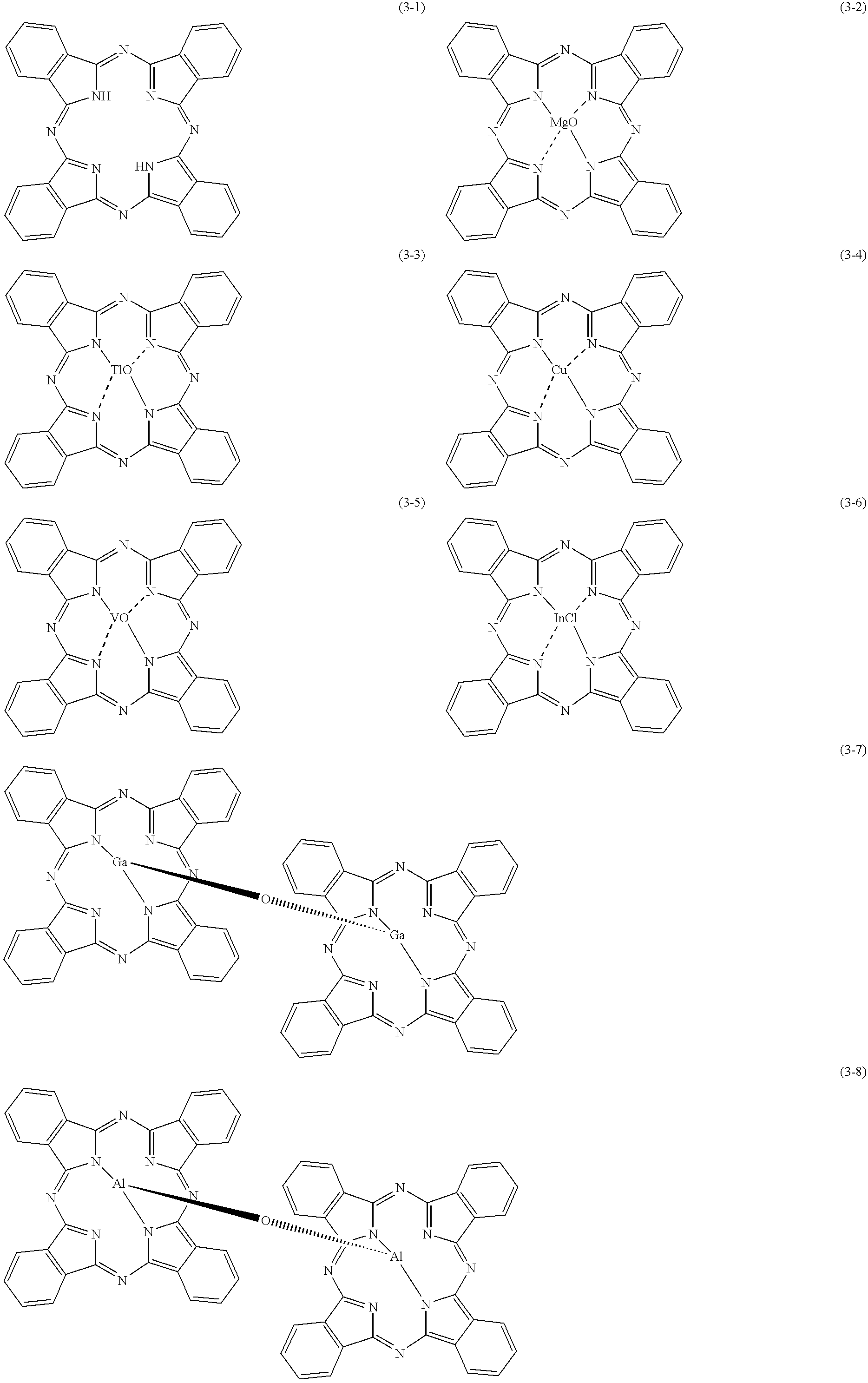
A charge generation layer with thickness of 0.2 .mu.m was formed on the undercoat layer by dip coating with a coating liquid and drying for 30 min at 80.degree. C. The coating liquid for the charge generation layer was prepared by dissolving and dispersing 1 part by weight of a charge generation material of titanylphthalocyanine and 1 part by weight of poly(vinyl butyr...

example 2

A photoconductor was produced in the same manner as in Example 1 except that the compound of the formula (5-3) was used as a charge transport material in place of the compound of the formula (5-11).

example 3

A photoconductor was produced in the same manner as in Example 1 except that the compound of the formula (5-4) was used as a charge transport material in place of the compound of the formula (5-11).


PUM

PropertyMeasurementUnit
wavelengthaaaaaaaaaa
light wavelengthaaaaaaaaaa

Abstract

A photoconductor includes a conductive substrate, an undercoat layer on the substrate, and at least one photosensitive layer on the undercoat layer. The radius of vacancy type defects in each of the photosensitive layer and in the undercoat layer is o.4 nm or less. In one embodiment, the radius of vacancy type defects is measured by a positron annihilation method.

Description

The present invention relates to an electrophotographic photoconductor (also called "a photoconductor") and, more specifically, to a relationship between an electrophotographic characteristic and the radius of the, vacancy type defects which are present in the functional layer of a photoconductor, in which the radius is a value measured by a positron annihilation method.Since the invention by Carlson disclosed in U.S. Pat. No. 2,297,691, numerous photoconductors have been developed including photoconductors using organic materials, such as phthalocyanines or azo compounds, as a charge generating material, as well as photoconductors using inorganic materials, such as amorphous silicon, a selenium-tellurium compound, or a selenium-arsenic compound.In particular, a printer, a digital copier, a facsimile machine, or a digital image-processing complex machine capable of combined functions of these machines, occasionally uses a semiconductor laser emitting at a wavelength of 635 nm to 780...

Claims


Application Information

Patent Timeline
Patent Type & Authority Patents(United States)
IPC IPC(8): G03G5/043G03G5/04G01N23/22G03G5/047G03G5/14
CPCG03G5/04G03G5/043
Inventor YAMAZAKI, MIKIONABETA, OSAMU
Owner FUJI ELECTRIC CO LTD
Why Eureka
Try Eureka