Ideal oxygen precipitating silicon wafers and oxygen out-diffusion-less process therefor

a technology of silicon wafers and oxygen precipitation, which is applied in the field of silicon wafer preparation, can solve the problems of affecting the operation of the device, contaminated with various impurities, and precipitates can be harmful or beneficial,

a technology of silicon wafers and oxygen precipitation, which is applied in the field of silicon wafer preparation, can solve the problems of affecting the operation of the device, contaminated with various impurities, and precipitates can be harmful or beneficial,

US6849119B2Inactive Publication Date: 2005-02-01SUNEDISON SEMICON LIMITED UEN201334164H

Image

  • Ideal oxygen precipitating silicon wafers and oxygen out-diffusion-less process therefor
  • Ideal oxygen precipitating silicon wafers and oxygen out-diffusion-less process therefor
  • Ideal oxygen precipitating silicon wafers and oxygen out-diffusion-less process therefor

Examples


examples 1 through 4

illustrate the ideal oxygen precipitation process of the present invention. These Examples should therefore not be interpreted in a limiting sense.

example 1

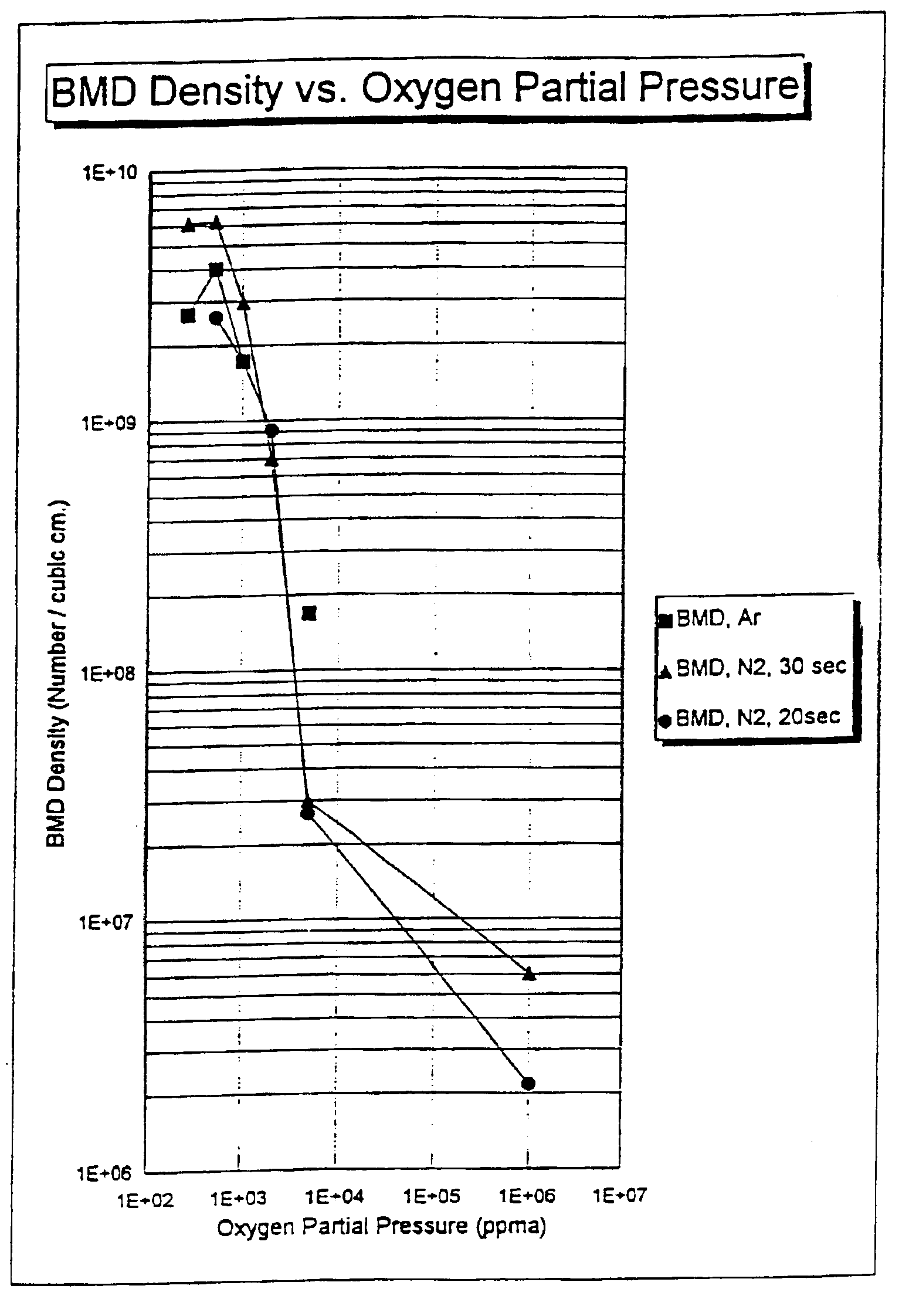
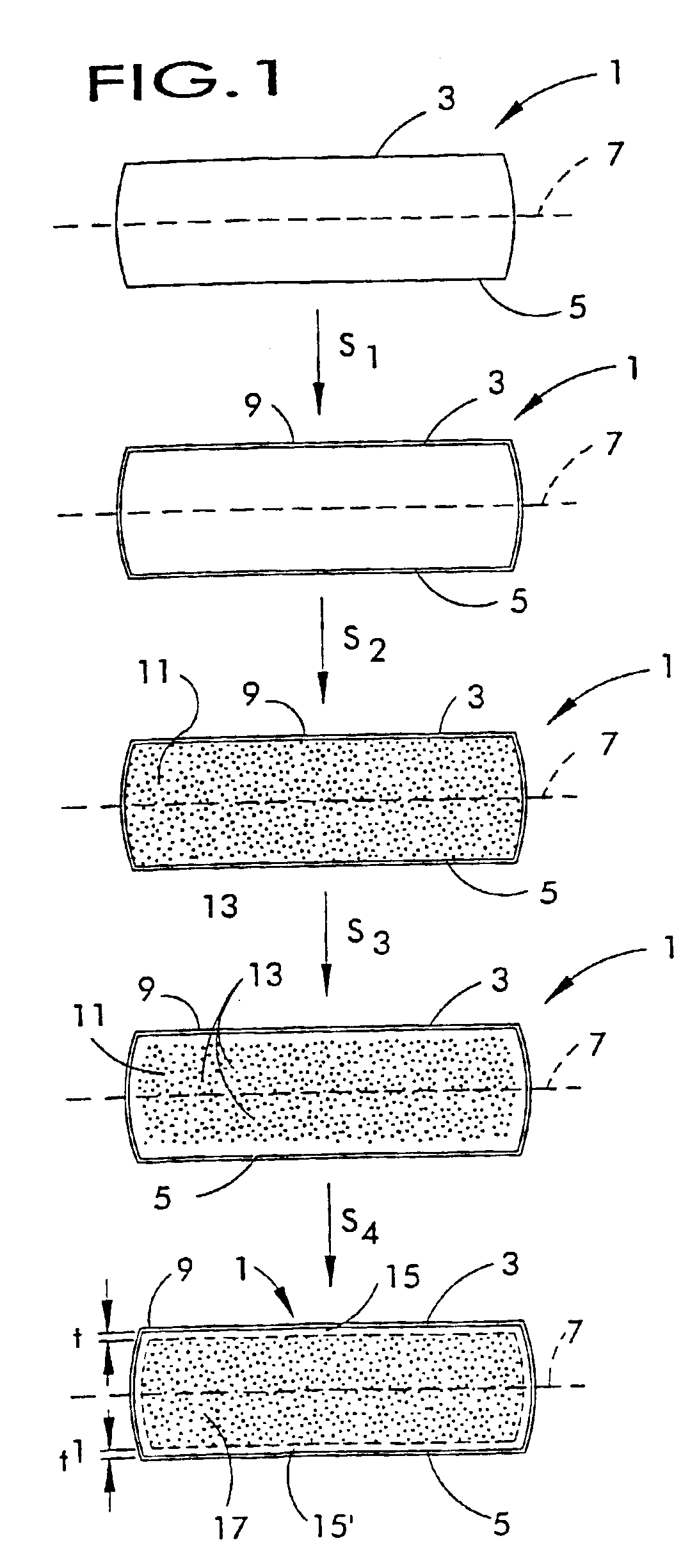
Silicon single crystals were pulled by the Czochralski method, sliced and polished to form silicon wafers. These wafers were then subjected to a surface oxidation step (S1), rapid thermal annealing step in nitrogen or argon (S2), rapidly cooled (S3), and subjected to an oxygen stabilization and growth step (S4) under the conditions set forth in Table I. The initial oxygen concentration of the wafers (Oi) before steps S1-S4, the oxygen precipitate density in the bulk of the wafers after step S4 (OPD), and the depth of the denuded zone after step S4 (DZ) are also reported in Table I.

TABLE ISample4-74-83-14S115 min at15 min atnone1,000° C.1,000° C.in N2 +in N2 +˜1% O2˜1% O2S235 seconds35 seconds35 secondsat 1250° C.at 1250° C.at 1250° C.in N2in Arin N2S3100° C. / sec100° C. / sec100° C. / secS44 hr at4 hr at4 hr at800° C. +800° C. +800° C. +16 hr at16 hr at16 hr at1,000° C.1,000° C.1,000° C.in N2in N2in N2Oi7 × 10176.67 × 1017 7.2 × 10¹⁷(atoms / cm3)OPD1 × 1010 4.4 × 10⁹ 1.69 × 10¹⁰(atoms / cm3)...

example 2

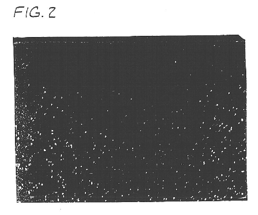
To demonstrate that the process of the present invention is relatively independent of oxygen concentration for Czochralski-grown silicon wafers, three wafers having different oxygen concentrations were subjected to the same series of steps described in Example 1. The conditions for each of these steps, the initial oxygen concentration of the wafers (Oi) before steps S1-S4, the oxygen precipitate density (OPD) in the bulk of the wafers after step S4, and the depth of the denuded zone (DZ) after step S4 as measured from the surface of the wafer are reported in Table II. FIGS. 6, 7, and 8 show cross-sections of the resulting wafers (these figures are enlargements of photographs taken at a magnification of 200×); sample 3-4 is shown in FIG. 6, sample 3-5 is shown in FIG. 7, and sample 3-6 is shown in FIG. 8.

TABLE IISample3-43-53-6S115 min at15 min at15 min at1,000° C.1,000° C.1,000° C.in N2 +in N2 +in N2 +˜1% O2˜1% O2˜1% O2S235 seconds35 seconds35 secondsat 1250° C.at 1250° C.at 1250° C...


PUM

PropertyMeasurementUnit
distance D2aaaaaaaaaa
temperatureaaaaaaaaaa

Abstract

A process for heat-treating a single crystal silicon wafer to influence the precipitation behavior of oxygen in the wafer in a subsequent thermal processing step. The wafer has a front surface, a back surface, and a central plane between the front and back surfaces. In the process, the wafer is subjected to a heat-treatment to form crystal lattice vacancies, the vacancies being formed in the bulk of the silicon. The wafer is then cooled from the temperature of said heat treatment at a rate which allows some, but not all, of the crystal lattice vacancies to diffuse to the front surface to produce a wafer having a vacancy concentration profile in which the peak density is at or near the central plane with the concentration generally decreasing in the direction of the front surface of the wafer.

Description

BACKGROUND OF THE INVENTIONThe present invention generally relates to the preparation of semiconductor material substrates, especially silicon wafers, which are used in the manufacture of electronic components. More particularly, the present invention relates to a process for the treatment of silicon wafers which enables the wafers, during the heat treatment cycles of essentially any arbitrary electronic device manufacturing process to form an ideal, non-uniform depth distribution of oxygen precipitates.Single crystal silicon, which is the starting material for most processes for the fabrication of semiconductor electronic components, is commonly prepared with the so-called Czochralski process wherein a single seed crystal is immersed into molten silicon and then grown by slow extraction. As molten silicon is contained in a quartz crucible, it is contaminated with various impurities, among which is mainly oxygen. At the temperature of the silicon molten mass, oxygen comes into the c...

Claims


Application Information

Patent Timeline
01 Feb 2005
Publication
US6849119B2
IPC
H01L21/02; H01L21/322; H01L21/26; C30B29/06
CPC
H01L21/3225; Y10T428/21; Y10S257/913; Y10T428/249969; H01L21/324
Inventors
FALSTER, ROBERT J.; CORNARA, MARCO