Methods of forming solder areas on electronic components and electronic components having solder areas

A technology of electronic components and solder, which is applied in the direction of assembling printed circuits, electrical components, and electrical components with electrical components, which can solve the problems of high labor intensity, high cost, and low output.

Inactive Publication Date: 2005-07-20
ROHM & HAAS ELECTRONICS MATERIALS LLC
View PDF2 Cites 12 Cited by
  • Summary
  • Abstract
  • Description
  • Claims
  • Application Information

AI Technical Summary

Problems solved by technology

The '742 patent further discloses that if the proportion of solder powder having a particle diameter of 20 μm or less is reduced, problems associated with its preparation, such as high labor intensity, low yield and high cost, are automatically ameliorated

Method used


Image

  • Methods of forming solder areas on electronic components and electronic components having solder areas
  • Methods of forming solder areas on electronic components and electronic components having solder areas
  • Methods of forming solder areas on electronic components and electronic components having solder areas

Examples


Embodiment 1-10

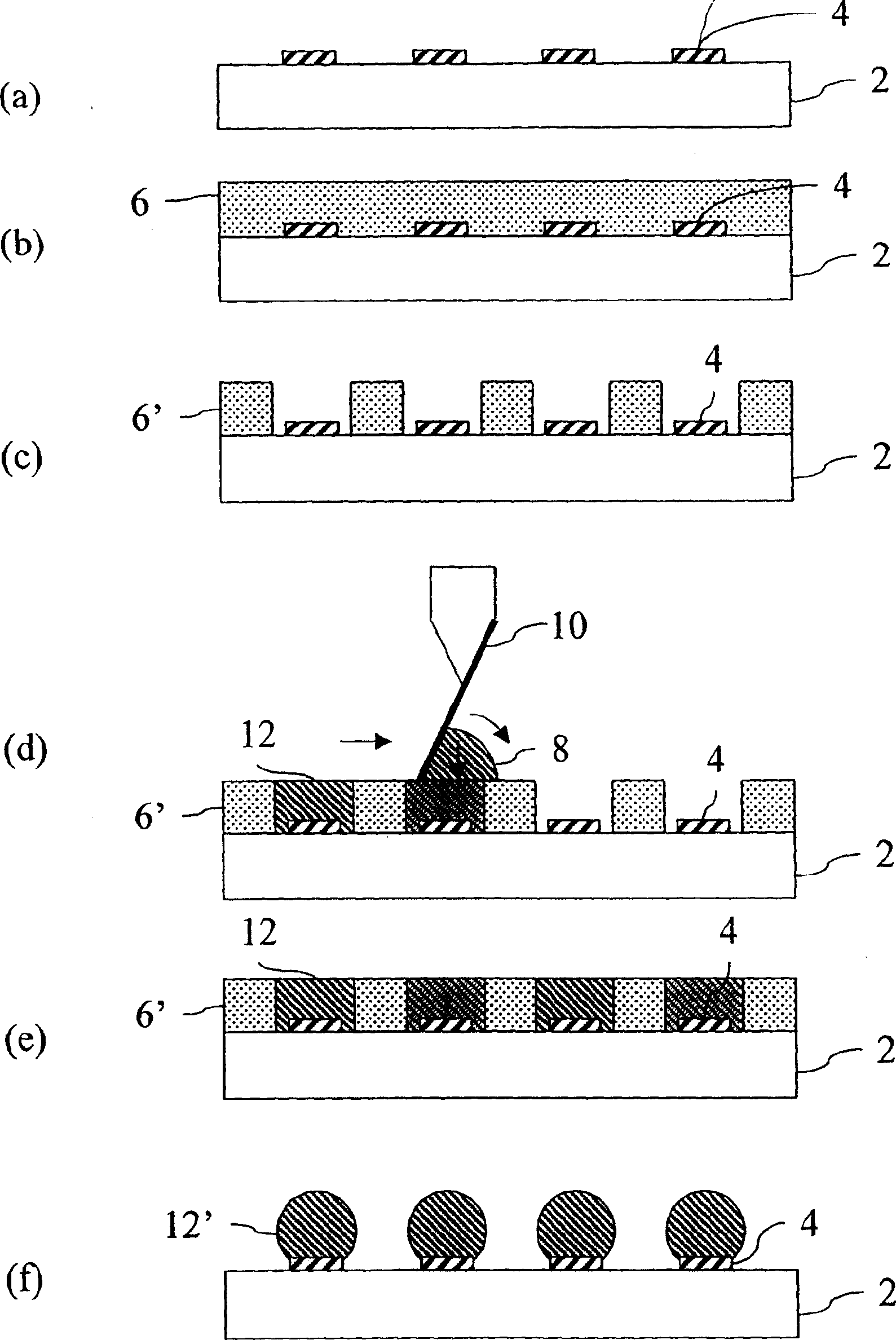
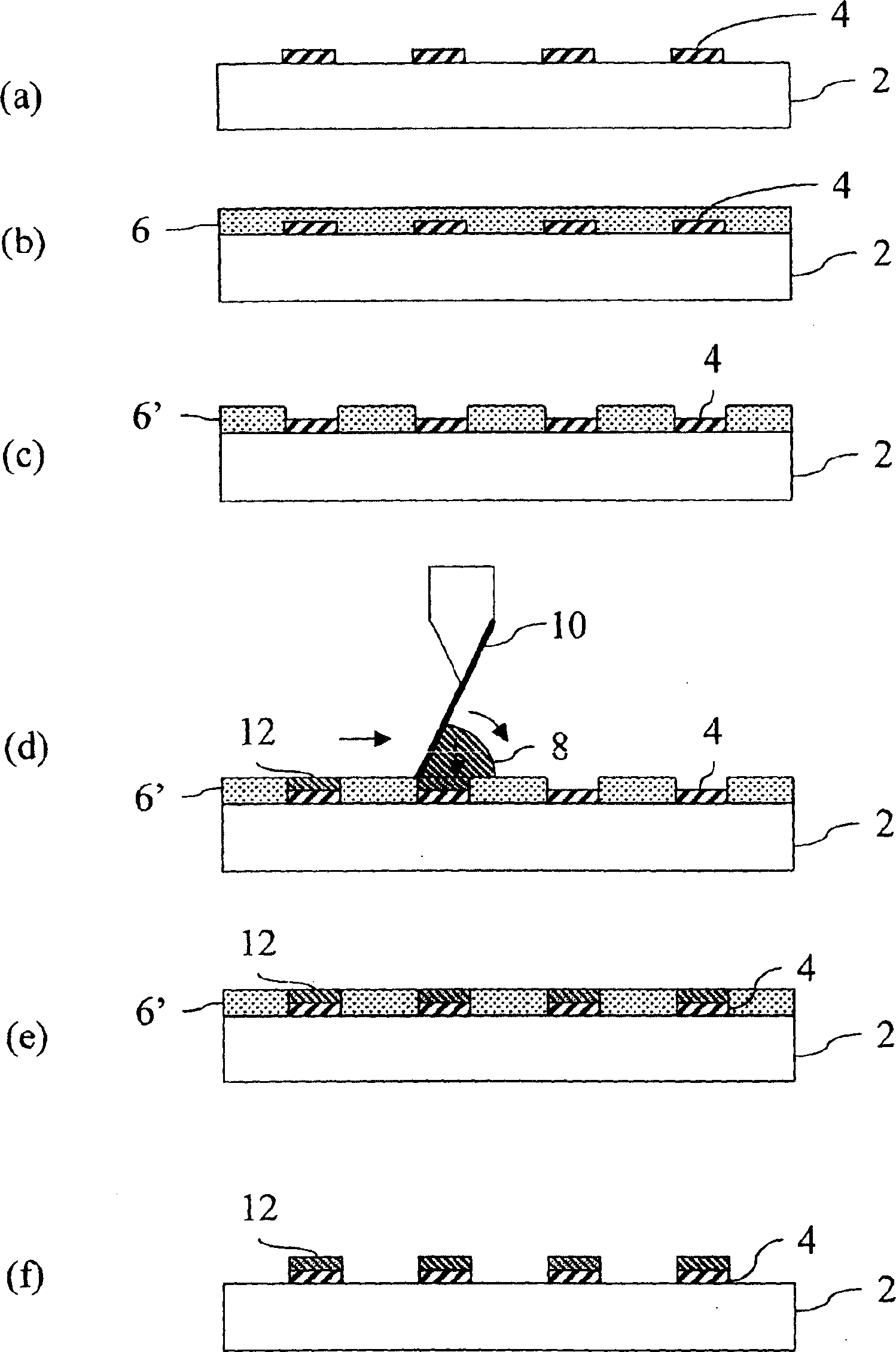
[0046] Nanoparticle solder pastes according to the present invention were prepared as follows. A 0.25 M solution of benzoic acid was prepared from 0.92 g of benzoic acid and 20 ml of diethyl ether. 86 g of solder alloy nanoparticles were added to the solution and soaked for one hour with occasional stirring. The powder slurry is rinsed and dried. A rosin-based flux was prepared from 50 wt% rosin, 41 wt% ethylene glycol solvent, 4 wt% succinic acid, and 5 wt% castor oil. The flux was added to the metal particles to form a paste with 88 wt% metal, as shown in Table 1. The resulting solder paste was used to form solder lands on electronic devices as described below.

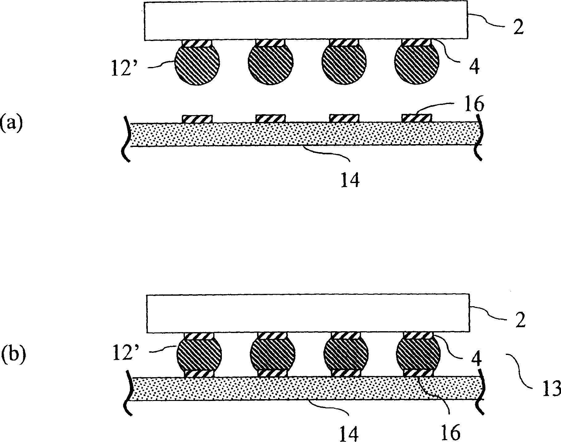
[0047] A semiconductor wafer having IC chips formed on its surface is provided. Each IC chip has 64 contact pads with a pitch of 100 μm (each side is 200 μm). A metal mask was placed in contact with the surface, the mask having openings with a diameter of 150 μm exposing the contact pads. Use the squeegee to s...


PUM

PropertyMeasurementUnit
diameteraaaaaaaaaa
diameteraaaaaaaaaa
diameteraaaaaaaaaa

Abstract

Disclosed are methods of forming solder areas on electronic components. The methods involve: (a) providing a substrate having one or more contact pads; and (b) applying a solder paste over the contact pads. The solder paste includes a carrier vehicle and a metal component having metal particles. The solder paste has a solidus temperature lower than the solidus temperature that would result after melting of the solder paste and resolidification of the melt. Also provided are electronic components which can be formed by the inventive methods. Particular applicability can be found in the semiconductor industry in the formation of interconnect bumps on a semiconductor component, for example, for bonding an integrated circuit to a module circuit or printed wiring board using a bump bonding process.

Description

[0001] Cross-references to related applications [0002] This application claims the benefit of US Provisional Application No. 60 / 532,264, filed December 22, 2003, under 35 U.S.C § 119(e), the entire contents of which are incorporated herein by reference. technical field [0003] The present invention relates to methods of forming solder areas on electronic components. At the same time, the invention relates to electronic components having solder regions. It can find specific application in the semiconductor industry in forming interconnection bumps on semiconductor devices, such as using solder bump connection processes to connect integrated circuits (ICs) to module circuits, interposers, or printed Printed Circuit Board (PWB). Background technique [0004] The semiconductor manufacturing industry is currently focused on wafer level packaging (WLB). In wafer-level packaging, IC interconnects are fabricated en masse on a wafer, and complete IC modules can be built on the...

Claims


Application Information

Patent Timeline
Patent Type & Authority Applications(China)
IPC IPC(8): H01L21/60B23K3/06B23K31/02H05K3/00H05K3/12H05K3/34H05K13/04
CPCH01L2924/01032H01L2924/01046H01L2924/01082H01L2924/0105H01L2924/01049H01L2224/81801H01L2224/16H01L2924/01327H01L2924/01322H05K3/3463H01L2924/01029H01L2224/13099H01L2924/01022H01L2224/1147H05K2201/0257H01L24/11H01L2924/014H01L2924/01013H01L2924/01024H01L2924/0103H05K2203/043H01L24/81H01L2924/04941H01L2924/01047H01L2924/01079H05K3/3484H01L2924/14H01L2924/01005H01L2924/01033H01L2924/01006B23K3/0638H01L2924/01074H01L2924/01078H01L2924/01057H01L2924/01075B23K2201/40H01L2924/01051B23K2101/40H01L24/05H01L24/13H01L2224/05568H01L2224/05573H01L2224/05611H01L2224/05624H01L2224/05644H01L2224/05647H01L2224/05655H01L2224/05664H01L2224/05666H01L2924/12042H05K3/3485H01L2924/00H01L2924/00014H05K3/12
Inventor N·E·布雷斯M·P·托本
Owner ROHM & HAAS ELECTRONICS MATERIALS LLC
Why Eureka
Try Eureka