Gallium nitride compound semiconductor device and manufacturing method

一种半导体、化合物的技术,应用在氮化镓类化合物半导体装置及其制造领域,能够解决发光元件成本增加、降低差排密度、花费工夫等问题

Inactive Publication Date: 2005-08-24
NITRIDE SEMICON
View PDF0 Cites 27 Cited by
  • Summary
  • Abstract
  • Description
  • Claims
  • Application Information

AI Technical Summary

Problems solved by technology

Conventionally, for example, the ELO (Epitaxial Lateral Overgrowth) method or the method of growing a light-emitting layer on a sapphire substrate with grooves is used to reduce the dislocation density. It takes time and effort, and as a result, there is a problem that the cost of the light-emitting element increases.

Method used


Image

  • Gallium nitride compound semiconductor device and manufacturing method
  • Gallium nitride compound semiconductor device and manufacturing method
  • Gallium nitride compound semiconductor device and manufacturing method

Examples


no. 1 Embodiment approach

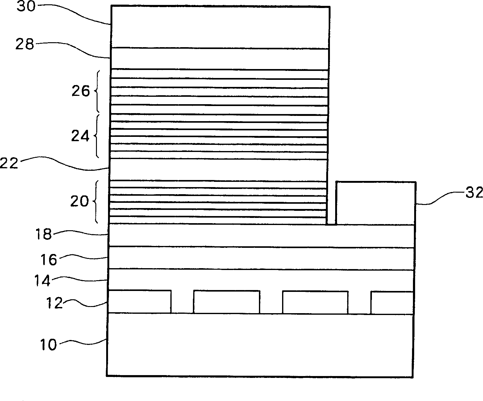
[0027] exist figure 1, shows the structure of a light-emitting element (LED (light-emitting diode)) that is the GaN-based compound semiconductor device of the present embodiment. A light-emitting element is manufactured by growing multiple layers on a substrate by MOCVD (Metal Organic Chemical Vapor Growth). Specifically, it was manufactured as follows. In addition, the MOCVD apparatus itself is known, but when the apparatus structure is outlined, a sensor and a gas introduction pipe are provided in a reaction tube. On the sensor, the substrate is placed, and the substrate is heated by the heater, and at the same time, the raw material gas is supplied, and the reaction proceeds on the substrate. The gas introduction part is provided, for example, on two sides of the reaction tube. One side introduces raw material gas such as trimethylgallium or silane gas from the side of the substrate, and the other side starts from the top of the substrate and passes through the gas-permea...

no. 2 Embodiment approach

[0070] Even under visible light, characters or figures cannot be seen even if they are drawn with a commercially available black pen (highlighter pen). However, when ultraviolet rays are irradiated here, the drawn characters or figures appear. Colored black pens (colored patterns appear when irradiated with ultraviolet light) are also commercially available, but in order to reproduce the color, the wavelength of the irradiated ultraviolet light must be 400nm or less, more precisely, the wavelength must be 380nm or less. Conventionally, fluorescent black lights or mercury lamps have been used as light sources, but they have the disadvantages of large size, large power consumption, and increased power supply.

[0071] Therefore, when using figure 1 When the light emitting element device (LED) shown is used as a light source for image reproduction, it can also be driven by a small battery. The figures drawn by the black pen were irradiated with LEDs having peak wavelengths of 40...

no. 3 Embodiment approach

[0075] The light from the LED of this embodiment was irradiated on human skin for a short time, and its influence was investigated. LED light with a peak wavelength of 400nm (5mW), 385nm (3mW), and 372nm (1mW) was irradiated on the skin for 10 minutes to investigate changes in the skin (so-called tanning). As a result, almost no influence was found at the peak wavelength of 400nm (5mW), and a slight change was observed at 385nm (3mW). On the other hand, at 372nm (1mW), a clear trace was seen. This means that LEDs with a wavelength of 365-380nm cause tanning of the human body. Using this LED as a light source, a tanning device is manufactured. An apparatus for tanning only dots with a diameter of 5 mm and an apparatus for tanning lines by arranging LEDs on a straight line with a length of 3 cm were fabricated and tested. Either device was irradiated for 10 minutes to obtain a tan. In addition, skin damage was considered to occur when irradiated for 30 minutes or more.

[0...


PUM


Abstract

A light-emitting element using GaN. On a substrate (10), formed are an SiN buffer layer (12), a GaN buffer layer (14), an undoped GaN layer (16), an Si-doped n-GaN layer (18), an SLS layer (20), an undoped GaN layer (22), an MQW light-emitting layer (24), an SLS layer (26), and a p-GaN layer (28), forming a p electrode (30) and an n electrode (32). The MQW light-emitting layer (24) has a structure in which InGaN well layers and AlGaN barrier layers are alternated. The Al content ratios of the SLS layers (20, and 26) are more than 5% and less than 24%. The In content ratio of the well layer in the MQW light-emitting layer (24) is more than 3% and less than 20%. The Al content ratio of the barrier layer is more than 1% and less than 30%. By adjusting the content ratio and film thickness of each layer to a desired value, the light luminous efficiency for wavelength of less than 400 nm is improved.

Description

technical field [0001] The invention relates to a gallium nitride (GaN) compound semiconductor device and a manufacturing method thereof, in particular to the improvement of luminous efficiency. Background technique [0002] Light-emitting devices in the wavelength range of 370 to 550 nM using nitride semiconductors have been put into practical use. These light-emitting elements mainly use In x Ga 1-x N (0<x<1) is used as a luminescent material. By changing In x Ga 1-x The In component ratio in N changes the emission wavelength by x, and specifically, the larger x is, the longer the emission wavelength becomes. In addition, when the In composition ratio x is changed, the luminous wavelength and luminous efficiency also change together. Specifically, when the In composition ratio x becomes larger, it is due to (1) the difference in lattice constant between GaN or AlGaN that becomes a layer sandwiching InGaN becomes larger and (2) in order to have a high In composi...

Claims


Application Information

Patent Timeline
Patent Type & Authority Applications(China)
IPC IPC(8): H01L33/04H01L33/06H01L33/32
CPCH01L33/32H01L33/06H01L33/04B82Y20/00
Inventor 佐藤寿朗菅原智也北泽慎二村本宜彦酒井士郎
Owner NITRIDE SEMICON
Why Eureka
Try Eureka