Phosphorescent light-emitting component comprising organic layers

An organic layer and fluorescent technology, applied in the field of fluorescent emitting elements, can solve the problems of lowering OLED efficiency and failure to recombine

Inactive Publication Date: 2005-08-31
NOVALED GMBH
View PDF5 Cites 11 Cited by
  • Summary
  • Abstract
  • Description
  • Claims
  • Application Information

AI Technical Summary

Problems solved by technology

[0009] 4a, there may be a barrier layer, the hole side
[0011] 6a, there may be a barrier layer, the electronic side
However, B is a barrier material and thus cannot recombine radiatively from its triplet
This reduces the efficiency of the OLED

Method used


Image

  • Phosphorescent light-emitting component comprising organic layers
  • Phosphorescent light-emitting component comprising organic layers
  • Phosphorescent light-emitting component comprising organic layers

Examples


example 1

[0062] 1. Substrate,

[0063] 2. The bottom electrode, such as hole injection (anode),

[0064] 3. Hole injection layer,

[0065] 4. Hole Transport Layer (HTL),

[0066] 4a. If possible, there is a barrier layer on the hole side,

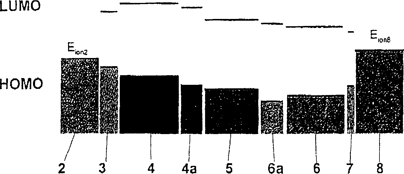
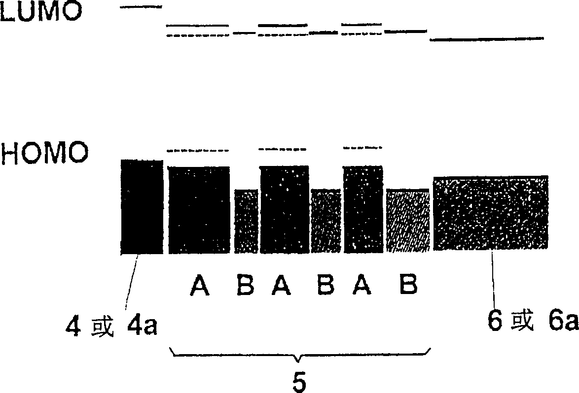
[0067] Light emitting area=multiple heterojunction (n=3)

[0068] 5A1d, hole transport material doped with emitter dopant (or bipolar transport material),

[0069] 5B1d or 5B1u, electron transport layer (or bipolar transport layer), may be doped with emitter dopants,

[0070] 5A2d, hole transport material doped with emitter dopant (or bipolar transport material),

[0071] 5B2d or 5B2u, electron transport layer (or bipolar transport layer), may be doped with emitter dopants,

[0072] 5A3d, hole transport material doped with emitter dopant (or bipolar transport material),

[0073] 5B3d or 5B3u, electron transport layer (or bipolar transport layer), may be doped with emitter dopants,

[0074] 6. Electron Transport Layer (ETL),

[0075] 7. Electron injectio...

example 2

[0081] 1. Glass substrate,

[0082] 2. ITO anode,

[0083] 4. Star-shaped (MTDATA) doped with F4-TCNQ 100nm (increased conductivity),

[0084] 4a. TPD (Triphenyldiamine), 5nm, HOMO=-5.4eV, LUMO=-2.4eV, light emitting area=multiple heterojunction (n=3)

[0085] 5A1d, Ir(ppy)3 doped TCTA used as a three-state emitter, 10nm,

[0086] 5B1u, BPhen 5nm

[0087] 5A2d, TCTA: Ir(ppy)3 15nm

[0088] 5B2u, BPhen 5nm

[0089] 5A3d, TCTA: Ir(ppy)3 2nm

[0090] 5B3u, BPhen 10nm

[0091] 6. Alq3 40nm

[0092] 7. LiF (lithium fluoride) 1nm,

[0093] 8. Aluminum (cathode).

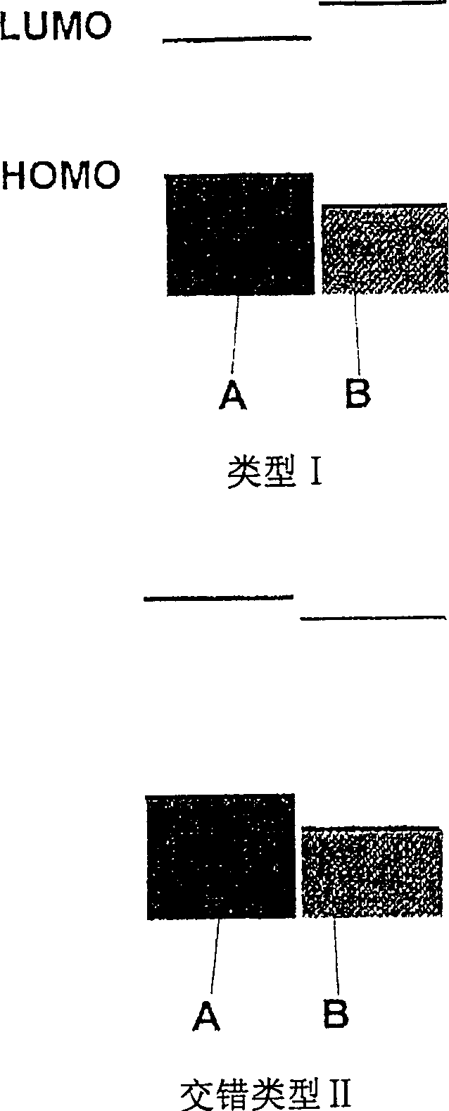
[0094] In this case, the interface AB is embodied, so that holes are blocked more effectively at the interface AB. This is necessary because only material A is doped with emitter dopants, and therefore there is a higher charge carrier density in material A. However, it is even more important that the three-state excitons in B have a greater energy than the energy in A. Therefore, the excitons generated on B can later be conver...

example 3

[0103] 1. Substrate,

[0104] 2. Bottom electrode, for example, ITO anode,

[0105] 3. Hole injection layer, such as phthalocyanine,

[0106] 4. Hole transport layer, such as MTDATA: F4-TCNQ,

[0107] 4a. The barrier layer on the hole side, such as TPD,

[0108] Light emitting area=multiple heterojunction (n=1)

[0109] 5AId, a hole transport layer doped with emitter dopants, such as TCTA: Ir(ppy)3,

[0110] 5B1d, electron transport layer and hole blocking layer doped with emitter dopants, such as Bphen:Ir(ppy)3,

[0111] 6a. The barrier layer on the electron side, such as BCP,

[0112] 6. Electron transport layer, such as Alq3,

[0113] 7. Electron injection layer, such as LiF,

[0114] 8. The top electrode (cathode), such as aluminum.

[0115] The formation of excitons in this OLED structure again occurs near the interfaces 5A1 and 5B1 (because the latter forms a "staggered II heterojunction"). The interface excitons can transfer their energy to the three-state excitons in the l...


PUM


Abstract

The invention relates to a light emitting component with organic layers and emission of triplet exciton states (phosphorescent light) with increased efficiency, having a layer sequence with a hole injecting contact (anode), one or more hole injecting and transporting layers, a system of layers in the light emission zone, one or more electron transport and injection layers and an electron injecting contact (cathode), characterized in that the light emitting zone comprises a series of heterojunctions with the materials A and B (ABAB . . . ) that form interfaces of the type 'staggered type II', one material (A), having hole transporting or bipolar transport properties and the other material (B) having electron transporting or bi-polar transport properties, and at least one of the two materials A or B being mixed with a triplet emitter dopant that is able to efficiently convert its triplet exciton energy into light.

Description

Technical field [0001] The present invention relates to a fluorescent emitting element having an organic layer, and in particular to an organic light emitting diode (OLED) according to the preamble of claims 1 and 2, which has an increased effect as a result of the new structure of the emitting region Current and quantum efficiency. Background technique [0002] Since the low operating voltage was confirmed by Tang et al. in 1987 (C.W. Tang et al. Appl. Phys. Lett. 51 (1987) 913), organic light-emitting diodes are allowed to be used as candidates for large-area displays. They consist of a series of thin layers (usually 1 nm to 1 μm) made of organic materials. These thin layers are preferably vapor-deposited in a vacuum (small molecule OLED) or applied from a solution, for example by spin coating (spin coating). -on) (Polymer OLED=PLED). After the electrical contact connection is made by the metal layer, the organic thin film forms different electronic or optoelectronic components...

Claims


Application Information

Patent Timeline
Patent Type & Authority Applications(China)
IPC IPC(8): H01L51/50
CPCH01L51/5016H10K50/11H10K2101/10C09K11/06Y10S428/917H10K50/15H10K50/16
Inventor 秦大山周翔杨·布鲁赫维兹-尼莫斯马丁·菲弗
Owner NOVALED GMBH
Why Eureka
Try Eureka