Method for producing a buried tunnel junction in a surface-emitting semiconductor laser

A surface emission and semiconductor technology, applied in the direction of semiconductor lasers, optical waveguide semiconductor structures, lasers, etc., to achieve high output, high single-mode performance, and stable horizontal single-mode operation

Inactive Publication Date: 2006-01-04
VERTILAS
View PDF1 Cites 0 Cited by
  • Summary
  • Abstract
  • Description
  • Claims
  • Application Information

AI Technical Summary

Problems solved by technology

Another disadvantage of this concept is the double epitaxy required for the overgrowth of the buried tunnel contact

Method used


Image

  • Method for producing a buried tunnel junction in a surface-emitting semiconductor laser
  • Method for producing a buried tunnel junction in a surface-emitting semiconductor laser
  • Method for producing a buried tunnel junction in a surface-emitting semiconductor laser

Examples


Embodiment Construction

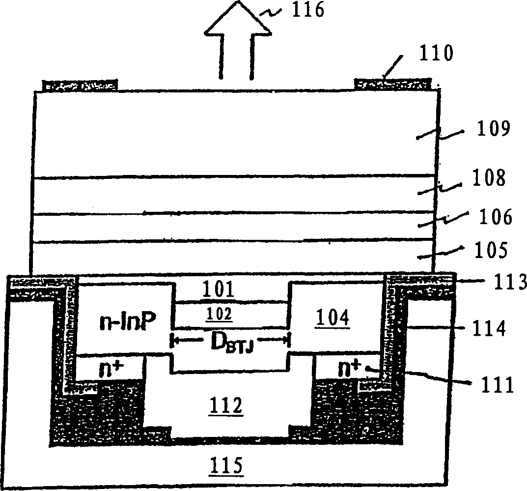
[0039] At the beginning of the manual, it is introduced according to the figure 1 Or 2's buried tunnel junction and the fabrication and structure of a surface-emitting laser diode with such a tunnel junction. Below, will refer to Figures 3 to 10 Embodiments of the present invention will be described in more detail.

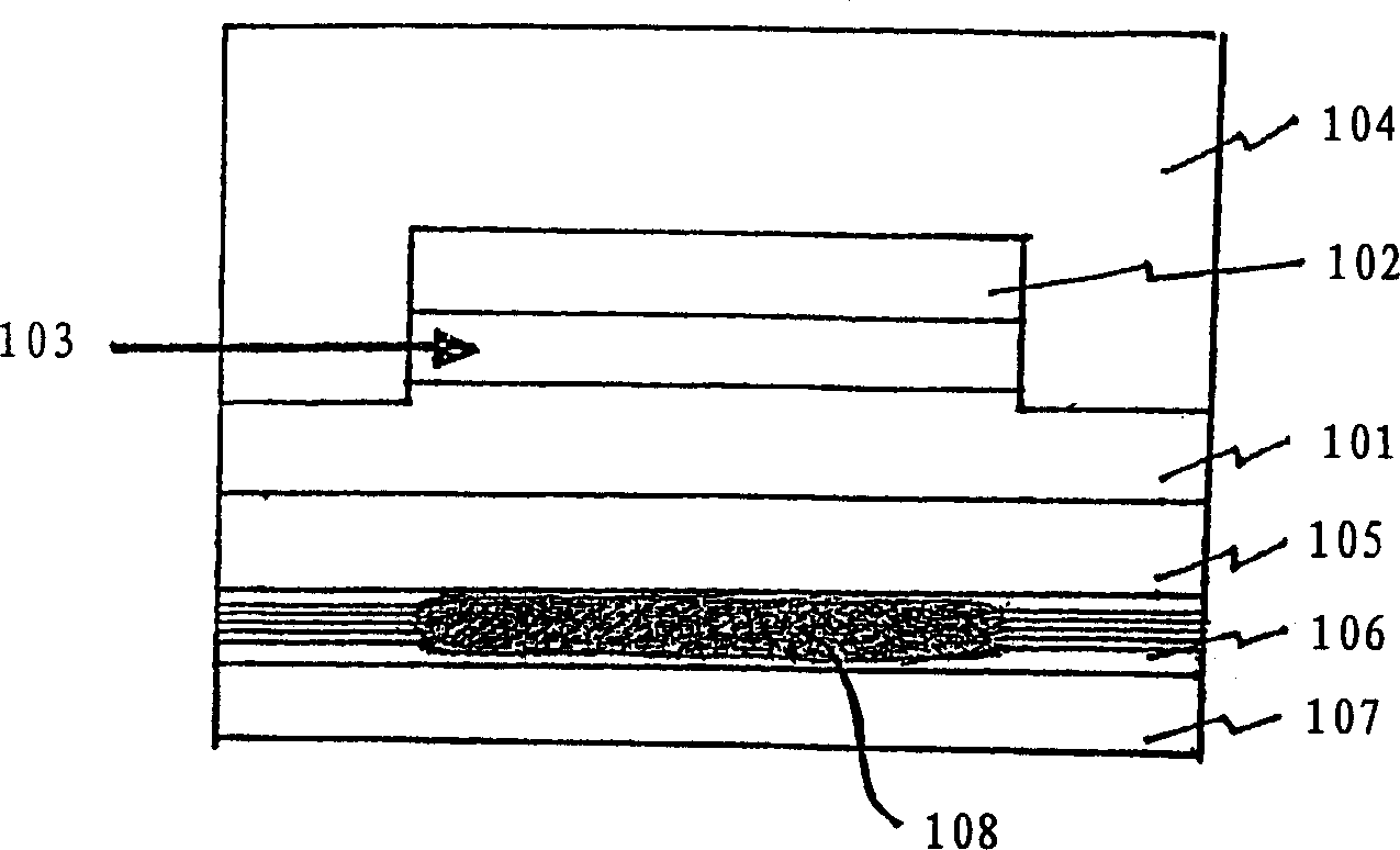
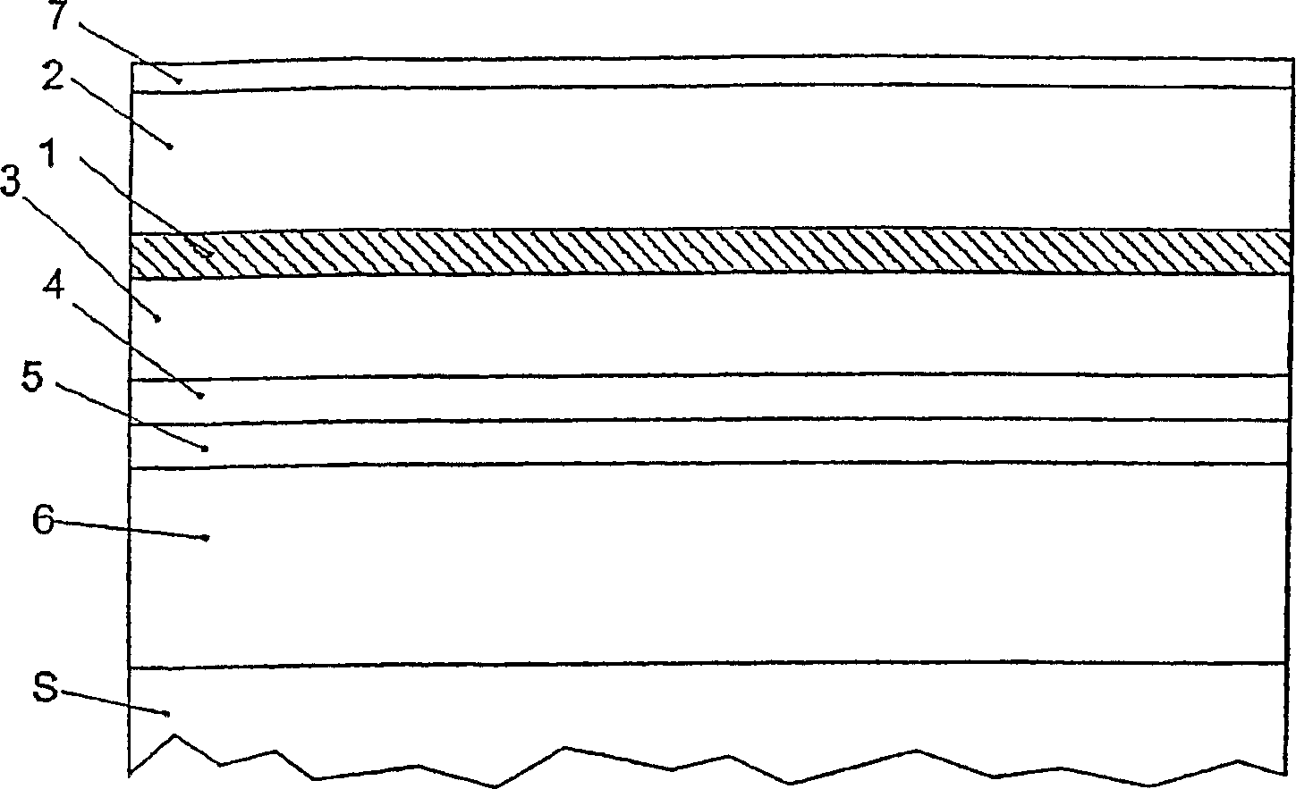
[0040] image 3 A general epitaxial initial structure for an MT-VCSEL according to the invention is schematically shown. Starting with an InP substrate S, sequentially deposit an n-doped epitaxial Bragg mirror 6, an active region 5, an optional p-doped InAlAs layer 4, a p-doped bottom InP layer 3, a wave junction in a longitudinal electric field (minimum) A tunnel junction 1 comprising at least one layer of each of highly p- and n-doped semiconductor layers, an n-doped upper InP layer 2, and n + The upper contact layer 7 is doped.

[0041] Next, through photolithography and etching, in accordance with the image 3 Circular or elliptical bumps (stamps) are f...


PUM


Abstract

The invention relates to a method for producing a buried tunnel junction (1) in a surface-emitting semiconductor laser and the laser of this type. The laser includes active area (5) containing pn junction enclosed by the first n doped semiconductor layer (6) and at least one p doped semiconductor layer (3, 4), and the tunnel junction (1) which is adjacent to the second n doped semiconductor on p side of the active area (5). To bury tunnel junction (1), the layer provided for the tunnel junction (1) is laterally stripped by material-selective in the first stage etching to the desired diameter of the tunnel junction. In the second stage, it is heated in a suitable atmosphere. This continues until the etched area (1a) is sealed by mass transfer from at least one semiconductor layer (2, 3) bordering on the tunnel junction (1). It makes it possible to produce a surface-emitting laser diode with simple technique in large yields, and enables steady work of cross single mode and high performance of the latter.

Description

technical field [0001] The invention relates to a method of manufacturing a buried tunnel junction in a surface emitting semiconductor laser and to a laser of this type. Background technique [0002] Surface-emitting laser diodes (in English: Vertical-Cavity Surface-Emitting Laser or VCSEL) are semiconductor lasers in which light emission occurs perpendicular to the surface of a semiconductor chip. Surface-emitting laser diodes have several advantages over conventional edge-emitting laser diodes, such as low electrical power consumption, direct inspection of laser diodes on wafers, simple coupling options with glass fibers, longitudinal single-mode spectroscopy, and the ability to work with Two-dimensional matrix interconnect surface-emitting laser diodes. [0003] In the field of optical fiber communication technology, VCSELs with a wavelength range of about 1.3 to 2 μm, especially around 1.31 μm to 1.55 μm, are required because of wavelength-dependent dissipation or absor...

Claims


Application Information

Patent Timeline
IPC IPC(8): H01S5/183H01S5/024H01S5/042H01S5/20H01S5/22H01S5/30H01S5/323
CPCH01S5/0425H01S5/18308H01S5/18369H01S5/024H01S2304/00H01S5/3235H01S5/3095H01S2301/176H01S5/02476H01S5/04253H01S5/04254H01S5/18377
Inventor 马库斯-克里斯琴·阿曼
Owner VERTILAS
Why Eureka
Try Eureka