

Power bipolar transistor with base local heavy saturation
A bipolar transistor and heavy doping technology, which is applied in the direction of transistors, semiconductor devices, electrical components, etc., can solve the problems of Auger recombination enhancement, emission zone doping band gap narrowing, and decline, so as to achieve performance improvement and improvement Effect of performance and current gain increase
- Summary
- Abstract
- Description
- Claims
- Application Information
AI Technical Summary
Problems solved by technology
Method used
Image

Examples
Embodiment Construction
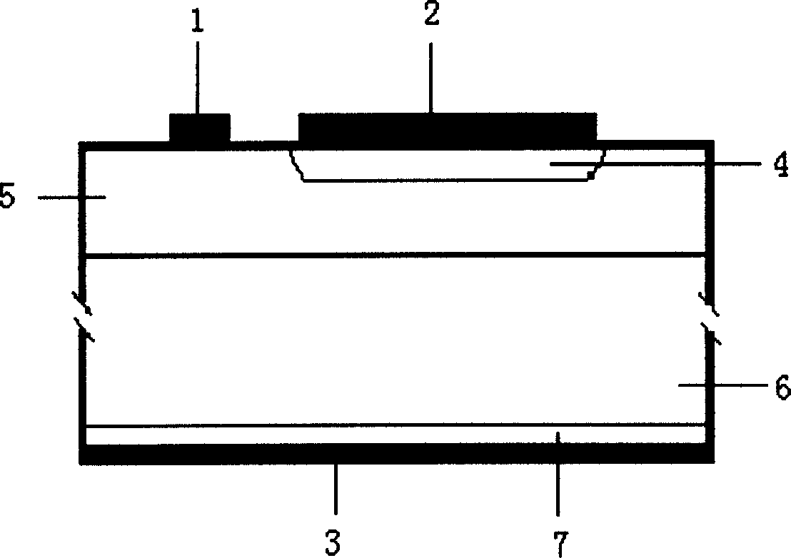
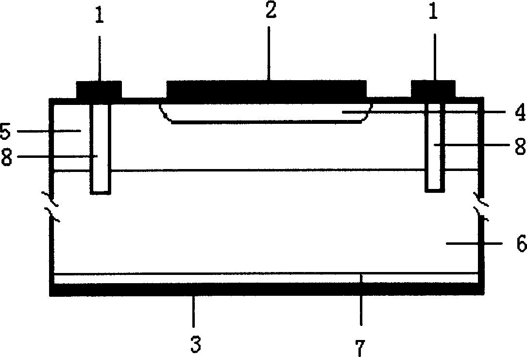
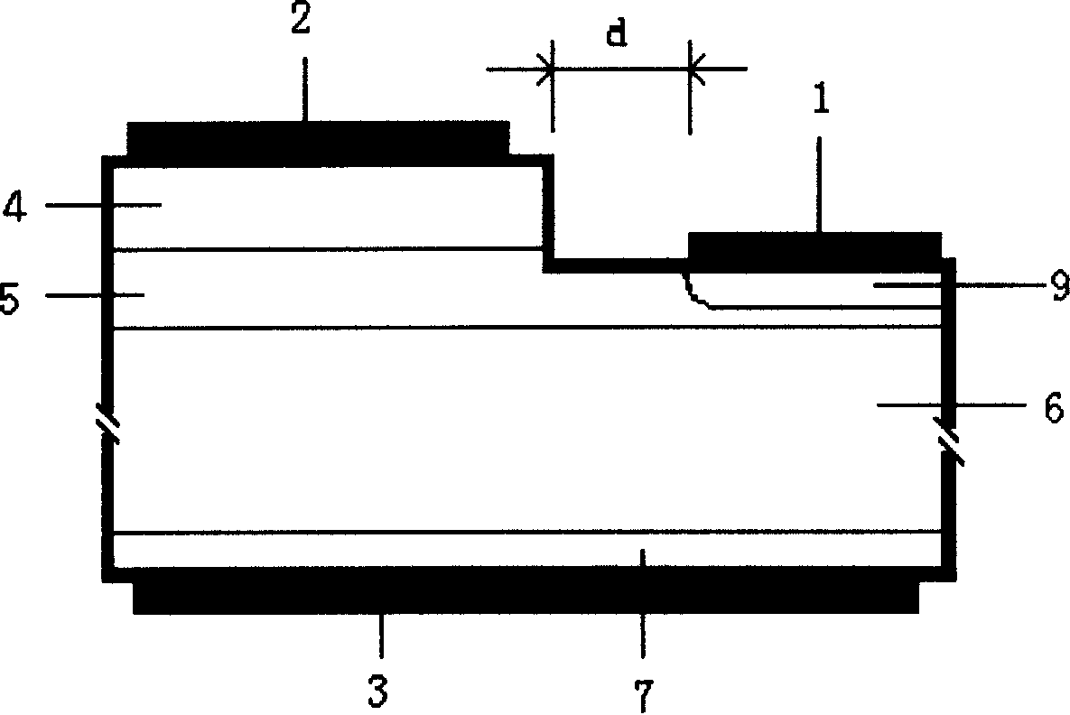
[0039] A kind of manufacturing process flow of the present invention has the local heavily doped power bipolar transistor in the base region as follows (taking the slot-type bipolar NPN transistor as an example):
[0040] 1) The wafer used is heavily doped N + Substrate 7;
[0041] 2) In heavily doped N + Fabricate N- / P / N sequentially on the substrate 7 + Epitaxial layer (different current gain and withstand voltage value of the device, the size of the epitaxial layer will be different);
[0042] 3) Etching away N by reactive ion etching (RIE) process + Layer to P layer, forming a groove structure of a bipolar transistor;
[0043] 4) forming a heavily doped base region 9 in the groove structure of the bipolar transistor according to the requirements of device current gain;
[0044] 5) Oxidation, forming a layer of high-quality oxide layer on the surface of the bipolar transistor tank;
[0045] 6) Deposit silicon dioxide, fill up the groove, and planarize the device;
[...
PUM
 Abstract
Description
Claims
Application Information