Supercharge Your Innovation With Domain-Expert AI Agents!

Array substrate for LCD and fabrication method thereof

A technology for liquid crystal displays and array substrates, used in semiconductor/solid-state device manufacturing, static indicators, instruments, etc., can solve problems such as reducing storage capacitance, increasing manufacturing costs, and degrading picture quality, and achieves a solution that reduces quantity and improves reliability. Effect

Inactive Publication Date: 2006-02-01
LG DISPLAY CO LTD
View PDF0 Cites 10 Cited by
  • Summary
  • Abstract
  • Description
  • Claims
  • Application Information

AI Technical Summary

Problems solved by technology

[0015] In addition, since the array substrate has a passivation layer on its entire surface including TFTs, expensive plasma-enhanced chemical vapor deposition (PECVD) equipment is generally required, which leads to an increase in manufacturing cost
[0016] In addition, since the passivation layer has a contact hole to connect the drain electrode and the capacitor electrode with the pixel electrode, the photolithography process for forming the contact hole is increased, which may increase the manufacturing cost and the risk of open failure of the data line
[0017] Product failure may occur due to the stepped portion of the contact hole during formation of the pixel electrode, and picture quality may deteriorate due to point defects
Also, if the passivation layer is not formed uniformly, it may reduce the storage capacitance, which may lead to spotty failures on the screen

Method used

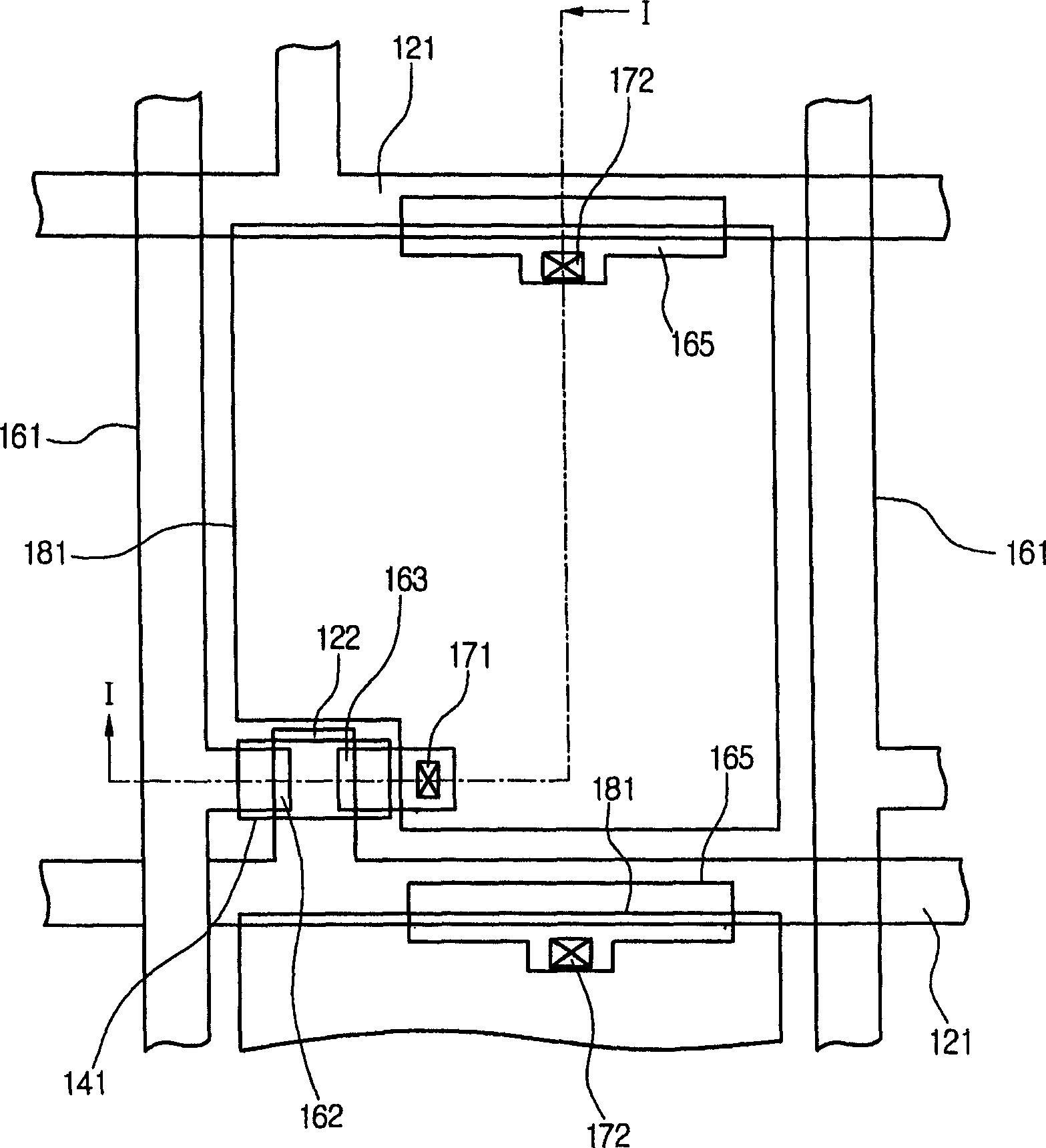
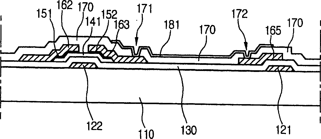

Image

  • Array substrate for LCD and fabrication method thereof
  • Array substrate for LCD and fabrication method thereof
  • Array substrate for LCD and fabrication method thereof

Examples


Embodiment Construction

[0038] Reference will now be made in detail to preferred embodiments of the invention, examples of which are illustrated in the accompanying drawings.

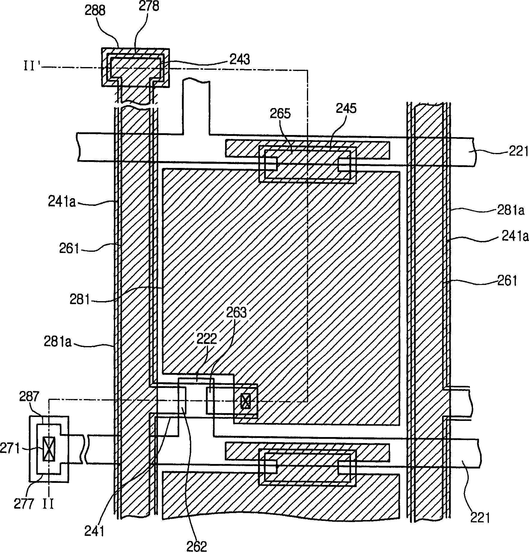
[0039] image 3 is a plan view of an LCD array substrate according to an embodiment of the present invention, Figure 4 is along image 3 The cross-sectional view taken by the line II-II'. refer to image 3 and 4 , the LCD array substrate includes: a transparent insulating substrate 210; a plurality of gate lines 221 formed on the transparent insulating substrate 210 along the horizontal direction; and a plurality of gates 222 protruding and extending from the plurality of gate lines 221 . A gate pad 277 is formed at one extended end of each of the plurality of gate lines 221 .

[0040] The first gate insulating layer 230 a having the gate pad contact hole 271 is formed on the gate pad 277 . A transparent electrode pattern 287 is formed on the first gate insulating layer 230 a, and the transparent electrode pattern 287 is el...


PUM


Abstract

Disclosed is an array substrate of an LCD, and a method for fabricating it, which simplifies the fabrication process, thereby reducing fabrication costs. The process is simplified because the array substrate does not have a passivation film. The thin film transistors on the array substrate each have an active layer that is protected from contamination by forming a channel insulation layer on the active layer through a dry-etching process. Further, the gate line, gate pad, and gate electrode may have a two-layer structure having a low-resistance metal layer and a barrier metal layer, or a three-layer structure having a low-resistance metal layer and two barrier metal layers.

Description

technical field [0001] The present invention relates to a liquid crystal display (LCD), and more particularly, to an LCD array substrate and a manufacturing method thereof, the method having fewer mask processes. Background technique [0002] As modern society rapidly shifts to an information-oriented society, demands for flat panel displays having superior performance advantages such as thin profile, light weight, and low power consumption and high-quality color reproduction have increased. A liquid crystal display (LCD), one of such flat panel displays, has been developed to meet this demand. [0003] Generally, an LCD includes two substrates each having electrodes formed on an inner surface. Two substrates are arranged to face each other, and a liquid crystal material is injected into a gap between the two substrates. LCDs display images by applying voltages to electrodes such that an electric field is generated within a liquid crystal material. The electric field cont...

Claims


Application Information

Patent Timeline
Patent Type & Authority Applications(China)
IPC IPC(8): G02F1/136G02F1/133H01L21/027H01L29/786G03F7/20G02F1/1362
CPCG02F1/1362G02F1/136213G02F1/13458G02F2001/13629G02F1/13629G02F1/1343G02F1/136
Inventor 崔荣锡安炳龙庾弘宇曹基述
Owner LG DISPLAY CO LTD
Features
  • R&D
  • Intellectual Property
  • Life Sciences
  • Materials
  • Tech Scout
  • Unparalleled Data Quality
  • Higher Quality Content
  • 60% Fewer Hallucinations
Learn More