Manufacturing process of MEMS impression template based on wet etching

A wet etching and manufacturing process technology, which is applied in the photoengraving process of pattern surface, photoengraving process coating equipment, semiconductor/solid-state device manufacturing, etc., can solve the problem of short etching resistance time and long metal layer deposition time. , etching and other problems, to improve the quality of the etched surface, eliminate surface defects, and reduce the undercut rate.

Inactive Publication Date: 2006-02-08
XI AN JIAOTONG UNIV
View PDF0 Cites 24 Cited by
  • Summary
  • Abstract
  • Description
  • Claims
  • Application Information

AI Technical Summary

Problems solved by technology

The traditional etching mask is photoresist + Cr / Au metal layer. Its process is mature, but the deposition time of the metal layer is long, the cost is high, and it is prone to "pinhole" etching defects
Deep etching can be done by using plasma-enhanced chemical vapor deposition (PECVD) polysilicon film or using a silicon wafer bonded to glass as an etching mask, but these methods are too expensive due to the complexity of the process
Using a double-layer Cr / Au metal layer plus a layer of 20μm photoresist as an etching mask can eliminate etching surface defects, but the process is more complicated
Using a single-layer photoresist as a mask has the advantages of simple process and low cost, but the problems of short etching resistance time and high undercut rate must be solved to obtain the required etching depth and sidewall steepness to meet the requirements of imprinting. needs

Method used


Image

  • Manufacturing process of MEMS impression template based on wet etching
  • Manufacturing process of MEMS impression template based on wet etching
  • Manufacturing process of MEMS impression template based on wet etching

Examples


Embodiment Construction

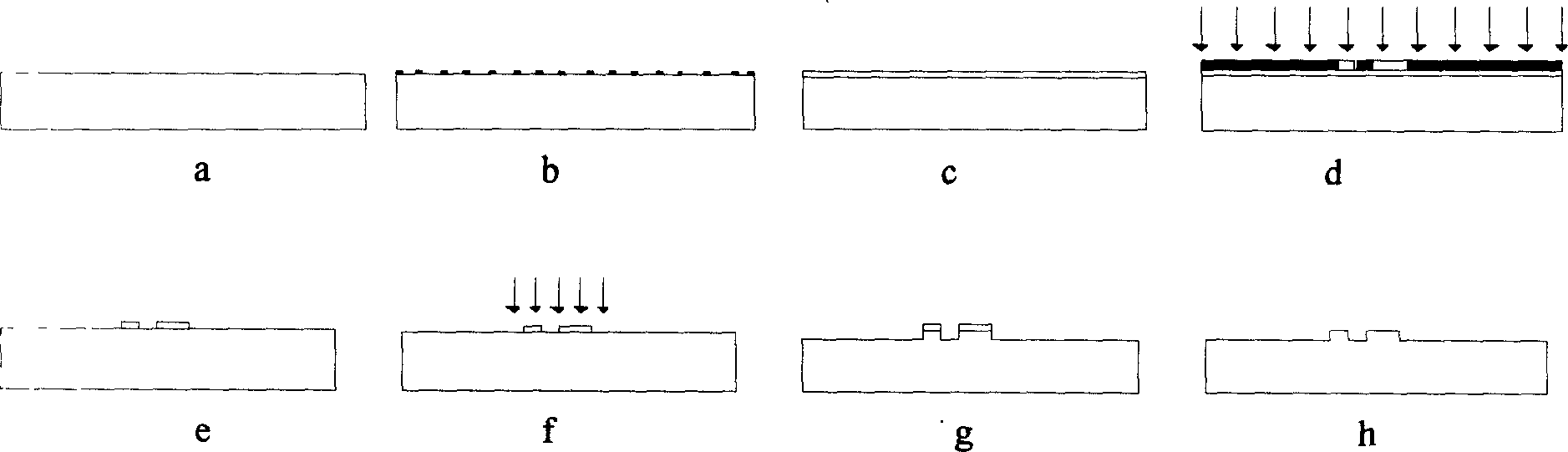
[0023] figure 1 For overall process flow diagram of the present invention, comprise the following steps:

[0024] Glass cleaning process ( figure 1 a) is: first wipe the glass with acetone, then rinse it with distilled water, soak the rinsed glass in concentrated sulfuric acid for 10 minutes; take it out, rinse it with distilled water, and dry it at 100°C for 10 minutes to remove the dirt on the glass ; Thorough cleaning can greatly reduce the etching defects caused by glass surface contamination.

[0025] After cleaning, adopt the mode of vapor deposition to carry out the spreading of silane coupling agent ( figure 1 b) The type of coupling agent used is KH-570. The coupling agent is used to improve the bonding force between photoresist and glass. The process of evaporating the coupling agent is: the temperature is 80°C, and the evaporation time is 30min , post-treatment after evaporation, the post-treatment method is to bake at 120 ° C for 40 minutes.

[0026] Next, glue...


PUM

PropertyMeasurementUnit
thicknessaaaaaaaaaa
thicknessaaaaaaaaaa
heightaaaaaaaaaa

Abstract

The invention discloses a product design for using glass wet method to etch the coining etch mold, which comprises: cleaning the base material, depositing coupling agent, coating etch glue, exposing, purging, doing second solid, etching, extracting the glue and so on to obtain the coining mold. The method adopts single layer negative photoresist as etching mask, it adopts silane coupling agent to enhance the adherence between the etching mask and the surface of the glass, it uses depositing mode to coat the coupling agent to reduce the drilling rate, and it adopts HCI as etching liquid agent to improve the etching surface quality. The method is suit for preparing MEMS.

Description

technical field [0001] The invention belongs to the field of microelectromechanical system (MEMS) manufacturing, and relates to a manufacturing process based on wet etching MEMS imprinting templates. The fabrication of imprint templates in the engraved MEMS layered manufacturing process can also be applied to the etching of microchannels in microfluidic analysis chips and the fabrication of optical components in micro-opto-electromechanical systems (MOEMS). Background technique [0002] Imprint lithography has proven to be a process capable of fabricating nanometer feature-sized structures, and has become a strong contender for next-generation lithography (NGL) due to its advantages of high precision, low cost, and suitability for mass production, and Some applications have been obtained. The production of imprint templates in imprint lithography is one of the key technologies. In room temperature imprint lithography, due to the requirements of expos...

Claims


Application Information

Patent Timeline
Patent Type & Authority Applications(China)
IPC IPC(8): G03F7/00G03F7/16G03F7/027G03F7/26H01L21/027
Inventor 段玉岗王权岱丁玉成洪军李涤尘卢秉恒
Owner XI AN JIAOTONG UNIV
Why Eureka
Try Eureka