Electronic component and electronic apparatus using this electronic component
A technology of electronic components and convex parts, applied in the direction of electrical components, impedance networks, etc., can solve the problem of insufficient attenuation of the receiver
- Summary
- Abstract
- Description
- Claims
- Application Information
AI Technical Summary
Problems solved by technology
Method used
Image

Examples
Embodiment approach 1
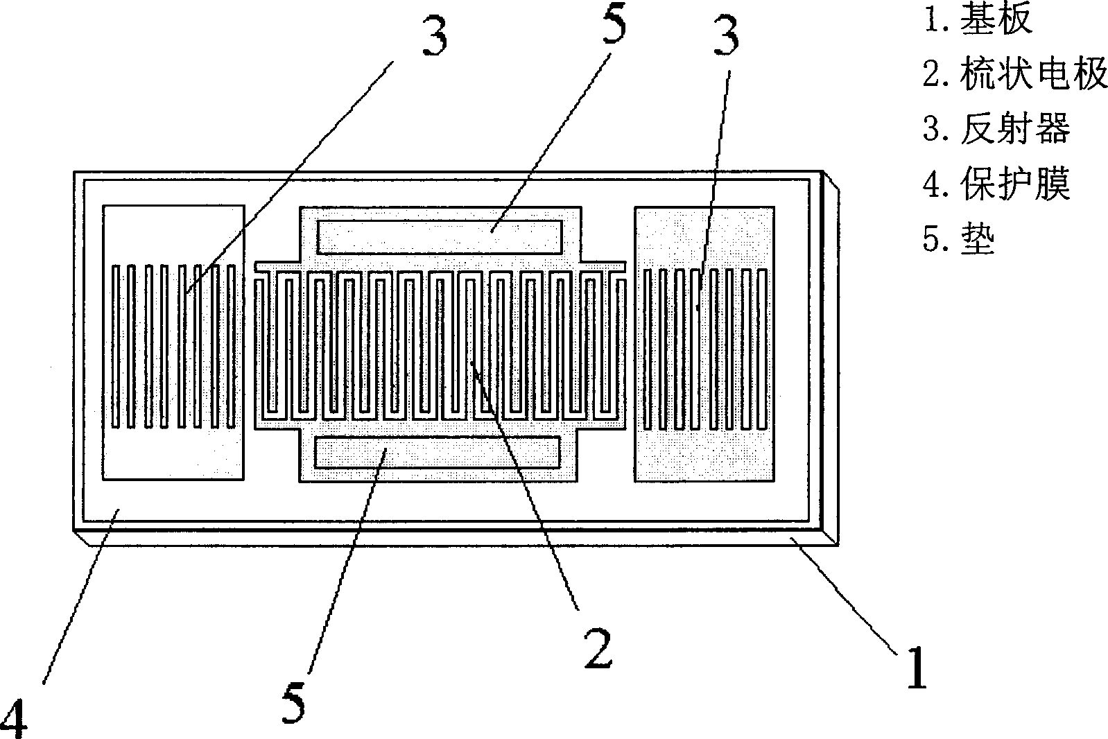
[0090] Figure 1A It is a top view of the SAW device as the electronic component of the first embodiment of the present invention, Figure 1B Is its cross-sectional view.
[0091] As shown in the figure, the SAW device of the first embodiment includes a comb-shaped electrode 2 on the substrate 1, a reflector 3 on both sides of the comb-shaped electrode 2, and at least covering the comb-shaped electrode 2 and the reflector 3 The protective film4. In addition, the comb-shaped electrode 2 is also provided with a pad 5 electrically connected to the comb-shaped electrode 2 for extracting electrical signals, thereby constituting a SAW device.
[0092] The substrate 1 is composed of a lithium-tantalate substrate (hereinafter referred to as "LT") cut out from the Y plate and rotated around the X axis at an angle of several degrees to the Z axis. The rotation angle is 36°. °YLT substrate.
[0093] The comb electrode 2 is made of aluminum (hereinafter referred to as "Al") or an Al alloy.
...
Embodiment approach 1
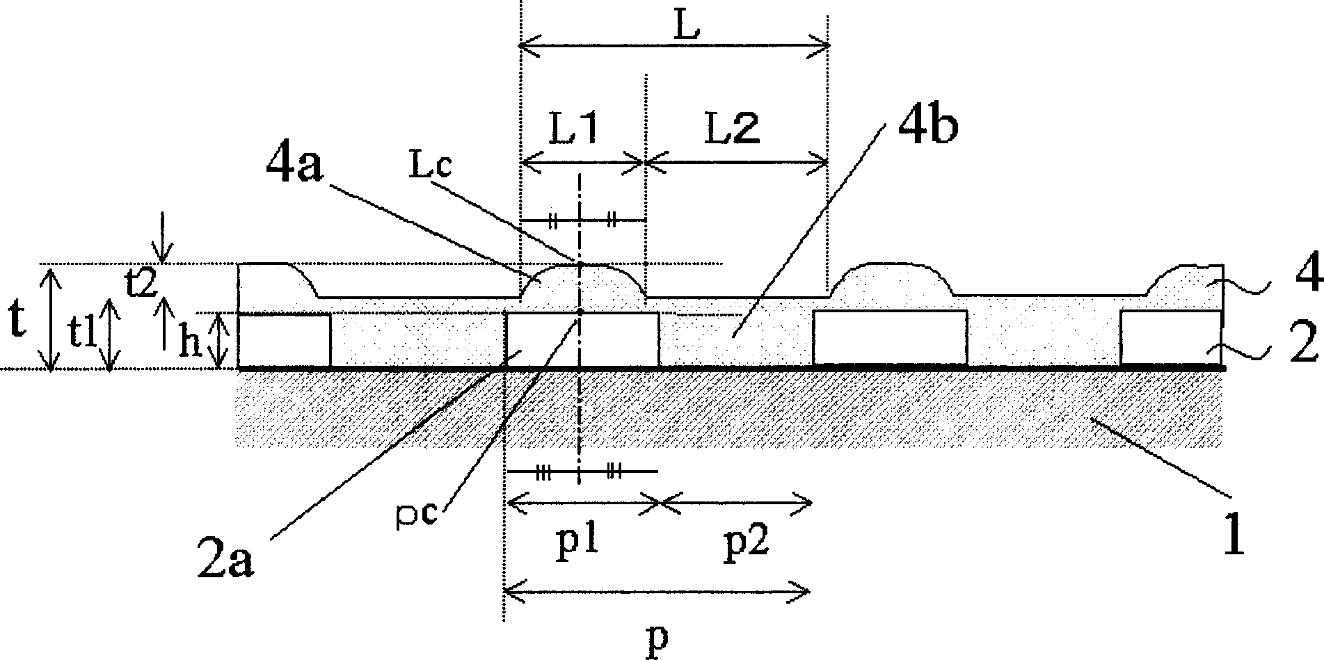
[0111] Embodiment 1 of the present invention satisfies
[0112] t2≤h (at this time, the relationship of Lp, p1+p2=p, L1+L2=L, L1≤p1, L2≥p2 is satisfied).
[0113] As a method of obtaining a shape satisfying this relationship, a so-called Bias sputtering method is used. This method is in the form of a manufacturing method schematic Figure 2E In the case of a SiO2 film, a bias is applied to the substrate side while the film is formed by sputtering. At this time, the shape of the SiO2 film can be controlled by changing the ratio of the bias voltage applied to the substrate and the sputtering power (power).
[0114] In this first embodiment, in order to show how to set the relationship between the height t2 from the top of the convex portion of the protective film to the bottom of the concave portion of the protective film and the film thickness h of the electrode, so that excellent characteristics can be obtained even when the protective film is formed. As the...
Embodiment approach 2
[0125] Hereinafter, the SAW device in Embodiment 2 of the present invention will be described with reference to the drawings.
[0126] The SAW device in the second embodiment uses the same SAW device as in the first embodiment. Picture 9 It is a cross-sectional view of a SAW device according to Embodiment 2 of the present invention. In this figure, the Figure 1B The same structure is marked with the same symbol, and its description is omitted.
[0127] The protective film 4 should be made of SiO2, such as Picture 9 As shown, it has an uneven shape on its top surface. The convex portion 94a of the protective film 4 is located above the portion having the comb-shaped electrode 2 on the upper surface of the substrate 1. On the other hand, the concave portion 94b of the protective film 4 is located between the convex portions 94a on the upper surface of the substrate 1 where there is no comb-shaped electrode 2 and its vicinity.
[0128] Here, it is assumed that the height from the ...
PUM
 Abstract
Description
Claims
Application Information