Transistor based on bibarrier tunnel junction resonance tunneling effect

A resonant tunneling and tunnel junction technology, applied in transistors, diodes, semiconductor devices, etc., can solve problems such as large leakage current, lack of control, and difficulty in fabricating double-barrier tunnel junctions

Active Publication Date: 2006-03-29
INST OF PHYSICS - CHINESE ACAD OF SCI
View PDF0 Cites 5 Cited by
  • Summary
  • Abstract
  • Description
  • Claims
  • Application Information

AI Technical Summary

Problems solved by technology

However, this type of transistor has the following disadvantages due to the Schottky potential between the base and the collector: ① lack of control over the base-collector potential energy; ② large leakage current at low emitter-base voltage; ③ Small collector current
However, due to the lack of research on the double-barrier tunnel junction and the difficulty of preparing a complete double-barrier tunnel junction, there is no spin transistor device based on the resonant tunneling effect of the double-barrier tunnel junction.

Method used


Image

  • Transistor based on bibarrier tunnel junction resonance tunneling effect
  • Transistor based on bibarrier tunnel junction resonance tunneling effect
  • Transistor based on bibarrier tunnel junction resonance tunneling effect

Examples


Embodiment 1

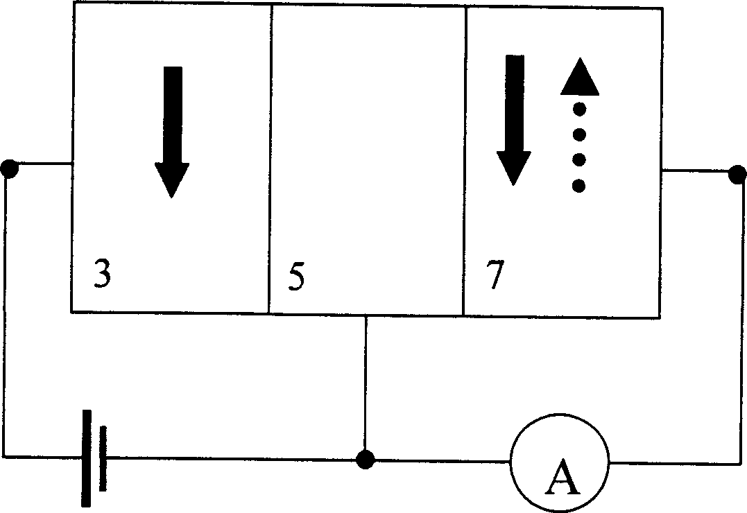
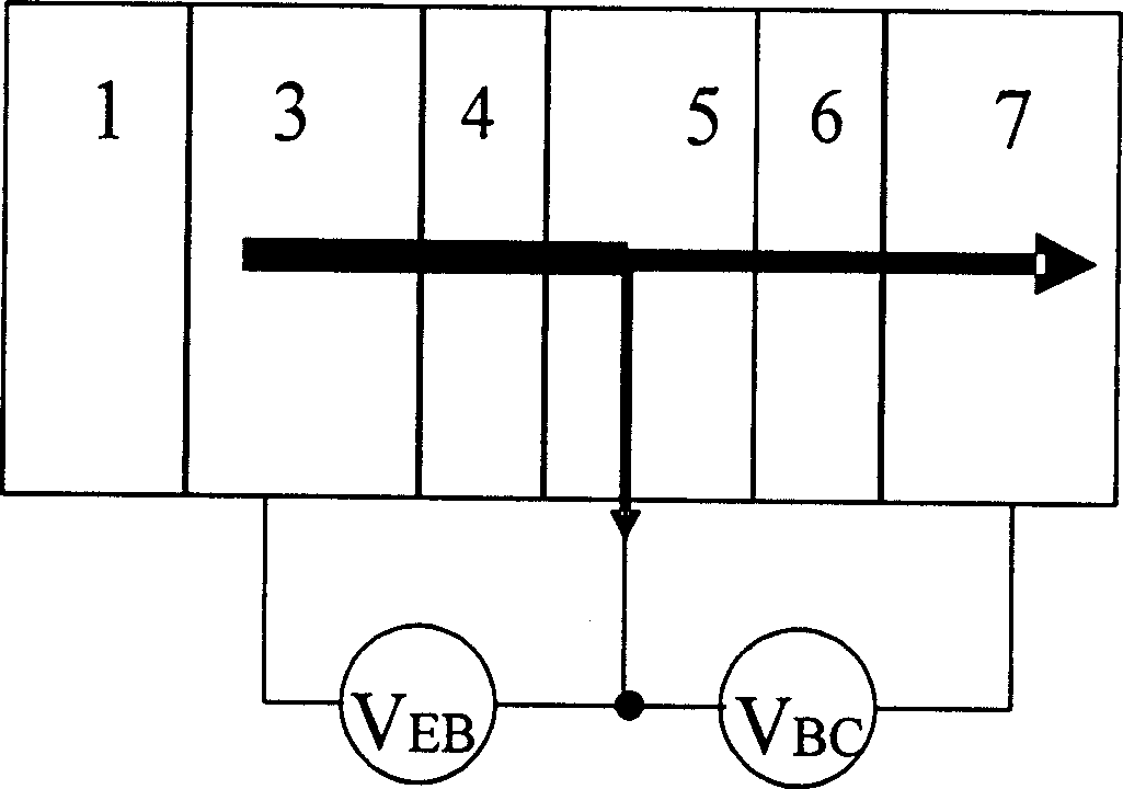
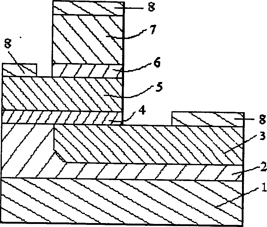
[0053] refer to Figure 3a and prepare a spin transistor with double potential barrier tunnel junction resonant tunneling effect of the present invention. The spin transistor with double potential barrier tunnel junction resonant tunneling effect is made of a Si material with a thickness of 0.4 mm as the substrate 1, and a layer of SiO is formed on the Si substrate 1. 2 An insulating layer 2 with a thickness of 10 nm is formed, and an emitter 3 is formed on the insulating layer 2. The emitter 3 is composed of an antiferromagnetic layer Ir-Mn with a thickness of 12 nm and Fe of 8 nm. The antiferromagnetic layer Ir-Mn is used for In the direction of the magnetization of the fixed emitter 3; using Al 2 o 3 The first tunnel barrier layer 4 made of materials is formed on the emitter 3; the thickness of the first tunnel barrier layer 4 is 1 nm. And a base 5 with a thickness of 8 nm is formed on the first tunnel barrier layer 4, and the base 5 is made of non-magnetic metal Cu. an...

Embodiment 2

[0056] refer to Figure 3a and prepare a spin transistor with double potential barrier tunnel junction resonant tunneling effect of the present invention. The spin transistor with double potential barrier tunnel junction resonant tunneling effect is made of a Si material with a thickness of 0.6 mm as the substrate 1, and a layer of SiO is formed on the Si substrate 1. 2 An insulating layer 2 with a thickness of 100 nm is formed, and an emitter 3 is formed on the insulating layer 2. The emitter 3 is composed of an antiferromagnetic layer Fe-Mn with a thickness of 15 nm and a La with a thickness of 4 nm. 0.7 Sr 0.3 MnO 3 The direction of the magnetization of the emitter 3 is fixed; SrTiO 3 The first tunnel barrier layer 4 made of material is formed on the emitter 3, and the thickness of the first tunnel barrier layer 4 is 1.0 nm; and a base electrode with a thickness of 4 nm is formed on the first tunnel barrier layer 4 5. The base 5 is composed of a non-magnetic metal mater...

Embodiment 3

[0060] refer to Figure 3a and prepare a spin transistor with double potential barrier tunnel junction resonant tunneling effect of the present invention.

[0061] The spin transistor with double potential barrier tunnel junction resonant tunneling effect is made of a Si material with a thickness of 0.6 mm as the substrate 1, and a layer of SiO is formed on the Si substrate 1. 2 An insulating layer 2 with a thickness of 300 nm is formed, and an emitter 3 is formed on the insulating layer 2, and the emitter 3 is composed of a GaMnAs magnetic semiconductor material layer with a thickness of 4 nm. The direction of the magnetization of the emitter 3 is relatively free and can change with the external magnetic field; the first tunnel barrier layer 4 made of MgO material is formed on the emitter 3; the first tunnel barrier layer 4 The thickness is 1.0 nm. And on the first tunnel barrier layer 4, a base electrode 5 with a thickness of 5nm is formed, and the base electrode 5 is made...


PUM


Abstract

The invention relates to a transistor based on the resonance tunneling effect of double-barrier tunnel junction, comprising: substrate, emitter, base, collector, and first and second tunnel barrier layers, where the first one is arranged between the emitter and base and the second one is between the base and collector; and the areas of tunnel junctions formed between the emitter and base and between the base and collector are 1 sq um-10,000 sq um; thickness of the base is comparable with free stroke of electrons of its material; only one of the emitter, base and collector has a free magnetization direction. Because of double barrier structure, the invention overcomes Schottky barrier generated between the base and collector, where the base current is modulation signal, and makes modulation modes of collector signal and base current similar by changing the magnetization direction of the base or collector, thus making the resonance tunneling effect, and can obtain an amplified signal on proper conditions.

Description

technical field [0001] The invention relates to a solid-state switch and amplifying device, that is, a transistor, especially a spin transistor device based on double potential barrier tunnel junction resonant tunneling effect. Background technique [0002] Since the discovery of the giant magnetoresistance effect (GMR) in magnetic multilayer films in 1988, great progress has been made in the research and application of physics and material science. In 1993, Johnson [M. Johnson, Science 260 (1993) 320] proposed a ferromagnetic metal emitter, a non-magnetic metal base with a thickness smaller than the spin diffusion length, and another ferromagnetic metal collector: " Ferromagnetic metal / nonmagnetic metal / ferromagnetic metal" sandwich all-metal spin transistor. figure 1 is a schematic diagram of this all-metal spin transistor. The speed of this all-metal transistor can be compared with that of semiconductor Si devices, but the energy consumption is 10-20 times lower, the de...

Claims


Application Information

Patent Timeline
Patent Type & Authority Applications(China)
IPC IPC(8): H01L29/70H01L29/72H01L29/88
Inventor 曾中明韩秀峰杜关祥魏红祥李飞飞詹文山
Owner INST OF PHYSICS - CHINESE ACAD OF SCI
Why Eureka
Try Eureka