Solid-state optical device

A technology of optical devices and solid-state components, which is applied in the fields of electrical solid-state devices, semiconductor/solid-state device components, semiconductor devices, etc., can solve the problems of high viscosity and solid-state optical devices without sealing performance, and achieve excellent moisture resistance.

Inactive Publication Date: 2006-05-03
TOYODA GOSEI CO LTD +1
View PDF4 Cites 2 Cited by
  • Summary
  • Abstract
  • Description
  • Claims
  • Application Information

AI Technical Summary

Problems solved by technology

[0009] However, the above-mentioned solid-state optical devices do not have sufficient sealing properties, even when low-melting glass sealing materials are used, because conventional low-melting glasses have high viscosity in the operating sealing temperature range

Method used


Image

  • Solid-state optical device
  • Solid-state optical device
  • Solid-state optical device

Examples


no. 1 approach

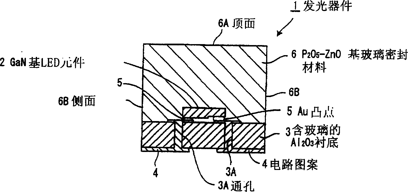
[0073] Figure 1A is a cross-sectional view showing a light-emitting device as a solid-state optical device in the first preferred embodiment of the present invention. Figure 1B is showing Figure 1A Side view of a GaN-based LED component.

[0074] [Configuration of Light-Emitting Device 1 ]

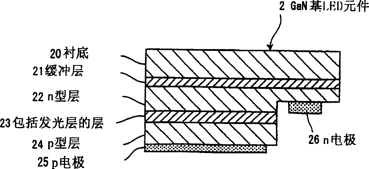
[0075] Figure 1A The light-emitting device 1 shown is composed as follows: a flip-chip type GaN-based LED element 2; 2 o 3 A substrate 3, which is an inorganic material substrate, on which a GaN-based LED element 2 is mounted; a circuit pattern 4, which is made of tungsten (W)-nickel (Ni)-gold (Au) and formed on a glass-containing Al 2 o 3 On the substrate 3; Au bump 5, which forms an electrical connection between the GaN-based LED element 2 and the circuit pattern 4; and a glass sealing material 6, which is P 2 o 5 -ZnO-Li 2 O-based transparent inorganic sealing material, and it is combined with glass-containing Al while sealing the GaN-based LED element 2 2 o 3 The substrate...

no. 2 approach

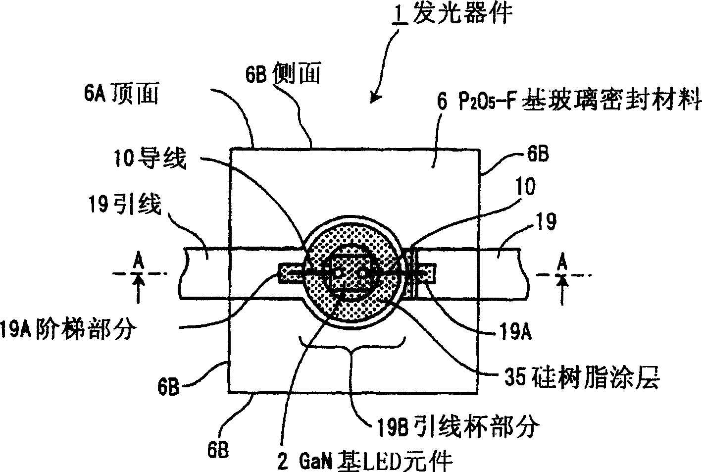
[0119] Figure 2A is a plan view showing a light emitting device as a solid-state optical device in the second preferred embodiment of the present invention; Figure 2B is along Figure 2A The cross-sectional view cut by the line A-A in; Figure 2C is showing Figure 2B Perspective view of the lower middle glass.

[0120] (Configuration of Light Emitting Device 1 )

[0121] The light emitting device 1 is composed as follows: a surface-mounted GaN-based LED element 2; a lead wire 19, as a power supply / recovery part, having a lead cover portion 19B on which the GaN-based LED element 2 is mounted; forming an electrical connection with the lead wire 19; and a silicone resin coating 35 covering the GaN-based LED element 2 and the wire 10 to protect them. GaN-based LED element 2 and leads 19 with P 2 o 5 -F-based glass sealing material 6 integrally sealed, the P 2 o 5 - The F-based glass sealing material 6 is composed of preformed upper glass 60A and lower glass 60B.

[01...

no. 3 approach

[0147] Figure 3A is a cross-sectional view showing a light-emitting device as a solid-state optical device in a third preferred embodiment of the present invention; Figure 3B is showing Figure 3A Side view of a GaN-based LED component.

[0148] (Configuration of Light Emitting Device 1 )

[0149] Figure 3A The light-emitting device 1 shown is composed of the following: a flip-chip GaN-based LED element 2 (the thermal expansion coefficient α is 5-7×10 -6 / °C); Al 2 o 3 A substrate 3, which is an inorganic material substrate, on which a GaN-based LED element 2 is mounted; a circuit pattern 4, which is made of tungsten (W)-nickel (Ni)-gold (Au), and formed on Al 2 o 3 On the substrate 3; Au bump 5, which forms an electrical connection between the GaN-based LED element 2 and the circuit pattern 4; and a glass sealing material 6, which is a transparent inorganic sealing material and bonded to Al 2 o 3 substrate 3 while sealing the GaN-based LED element 2 . In this emb...


PUM

PropertyMeasurementUnit
melting pointaaaaaaaaaa
glass transition temperatureaaaaaaaaaa

Abstract

PROBLEM TO BE SOLVED: To provide a solid-state element device in which an expected effect can be actually obtained by performing glass sealing after extracting and solving a problem for realizing inorganic material sealing work, further, humidity resistance is improved, and losing of transparency in glass sealing and cloudiness in characteristic evaluation do not occur.

SOLUTION: In a light emitting device 1 as a solid-state element device, a glass sealing part 6 is formed by performing hot press working of low fusing point glass of P<SB>2</SB>O<SB>5</SB>-ZnO-Li<SB>2</SB>O in a predetermined atmosphere for a glass containing Al<SB>2</SB>O<SB>3</SB>substrate 3 with a GaN LED element 2 mounted thereon. The glass sealing part 6 is worked at a temperature sufficiently lower than the crystal growth temperature of the GaN LED element 2. Thus, the light emitting device 1 can be obtained with humidity resistance and transparency and without occurrence of thermal element destruction.

COPYRIGHT: (C)2006,JPO&NCIPI

Description

[0001] This application is based on Japanese Patent Application Nos. 2004-263098, 2004-262908 and 2005-140284, the entire contents of which are incorporated herein by reference. technical field [0002] The present invention relates to solid-state optics, and more particularly, to solid-state optics with low-melting glass encapsulants. Herein, solid-state optical devices include various optical devices composed of solid-state elements (or semiconductor elements) such as light-emitting elements (or LED elements), light-receiving elements, and solar cell elements. Background technique [0003] In conventionally known solid-state optical devices, solid-state components such as LED components are encapsulated with a transparent resin material such as epoxy. Transparent resins are known to cause deterioration due to light exposure. In particular, when a Group III nitride-based compound semiconductor LED element emitting short-wavelength light is used, the transparent resin aroun...

Claims


Application Information

Patent Timeline
Patent Type & Authority Applications(China)
IPC IPC(8): H01L23/29H01L33/32H01L33/44H01L33/56H01L33/62
CPCH01L2224/48091
Inventor 末广好伸山口诚治沢登成人大塚正明渡部洋己相田和哉
Owner TOYODA GOSEI CO LTD
Why Eureka
Try Eureka