High resistance electromagnetic surface and preparation method thereof

An electromagnetic surface, high-resistance technology, applied in the direction of motor generator control, circuits, electrical components, etc., can solve the problems of reduced unit cell cycle number, discount, and excessive size of planar unit cells

Inactive Publication Date: 2006-06-14
SHANGHAI FANGSHENG INFORMATION TECH +1
View PDF0 Cites 5 Cited by
  • Summary
  • Abstract
  • Description
  • Claims
  • Application Information

AI Technical Summary

Problems solved by technology

Although the above-mentioned two types of planar electromagnetic bandgap structure materials can provide sufficient bandgap frequency width to meet the application needs of most microwave components, the size of the planar unit cell is still too large when the substrate adopts a dielectric carrier with a low dielectric constant. Due to the limited geometric size requirements of components, the nu

Method used


Image

  • High resistance electromagnetic surface and preparation method thereof
  • High resistance electromagnetic surface and preparation method thereof
  • High resistance electromagnetic surface and preparation method thereof

Examples


Embodiment 1

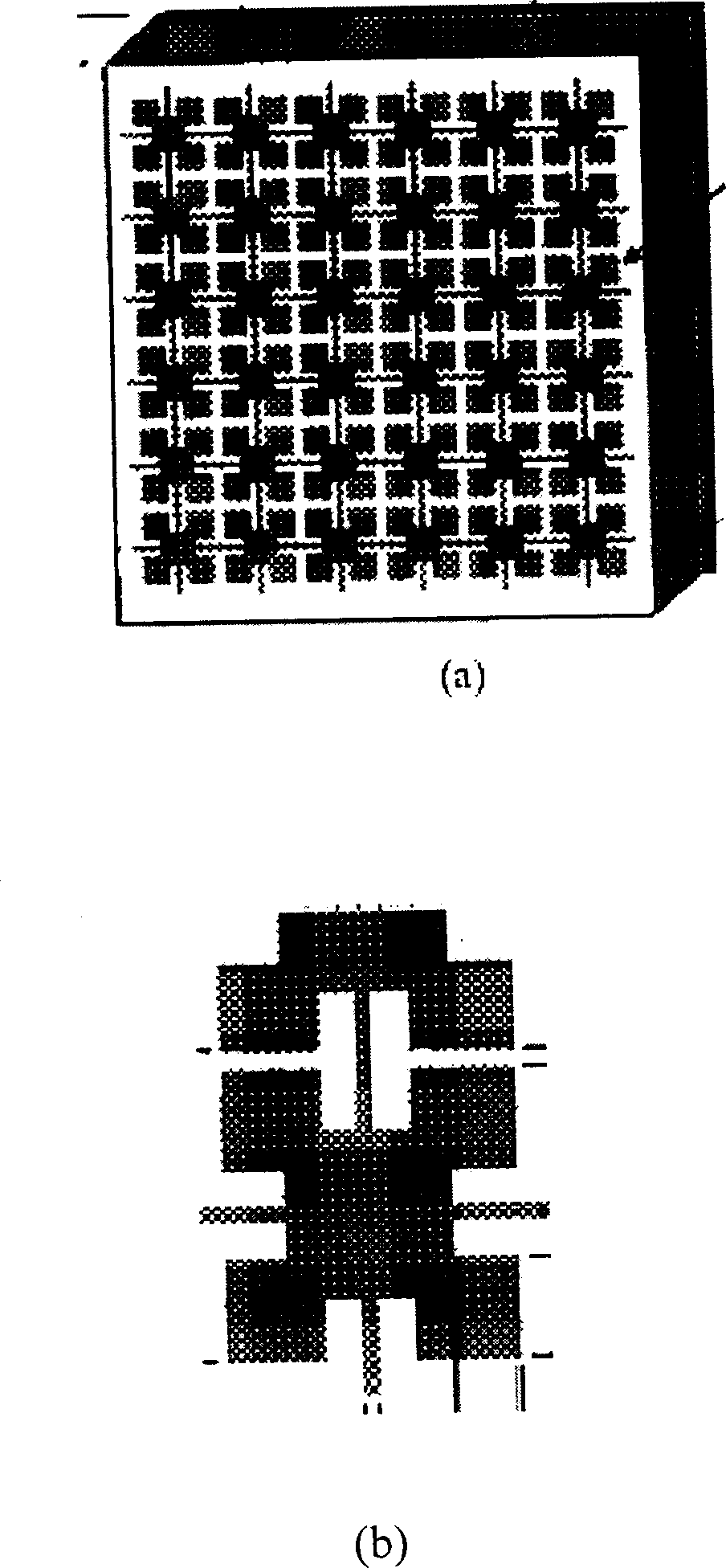
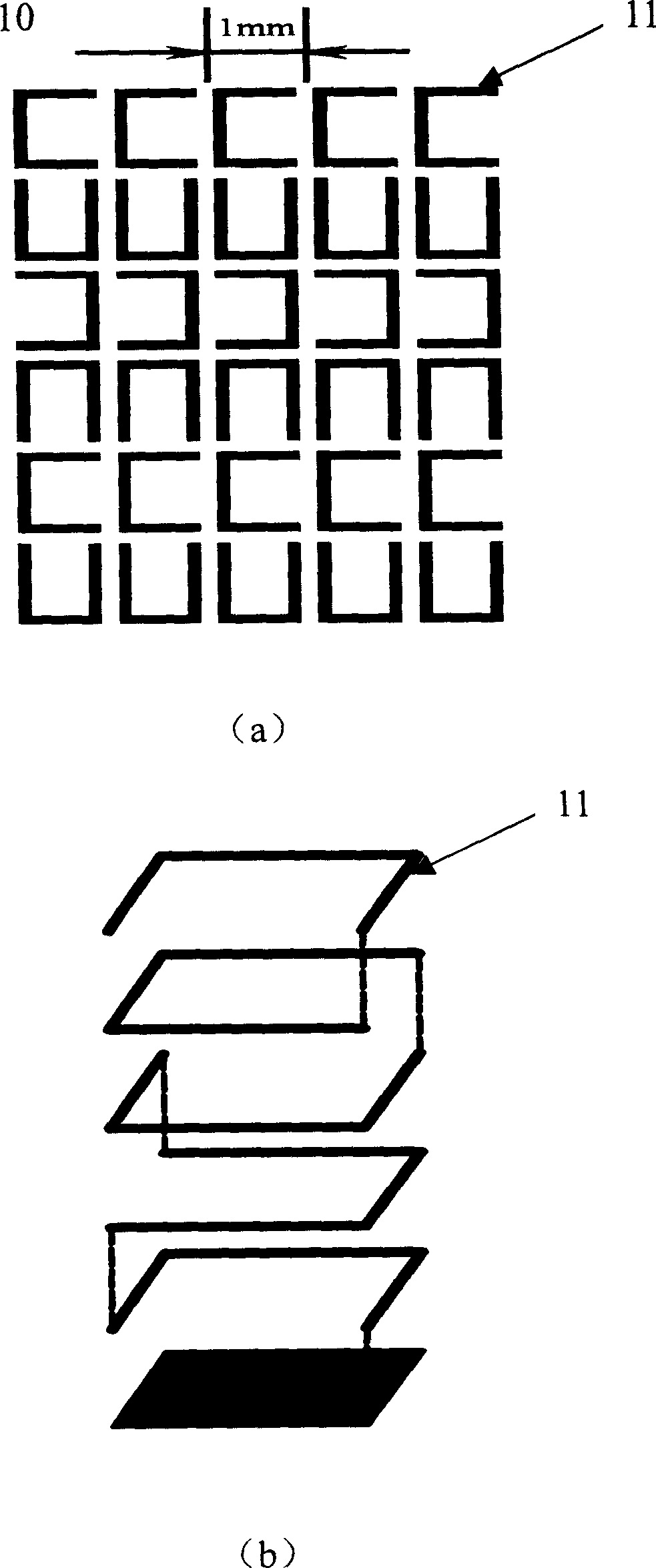
[0030] Example as image 3 As shown, the silver coils form a square, image 3 (a) is a top view of the first type of high-resistance electromagnetic surface 10, image 3 (b) is a schematic diagram of the structure of the square silver coil 11. Inside the first type of high-resistance electromagnetic surface 10, there are 7 layers of square silver coils 11. Some air gaps between the square silver coils 11 and the ceramic matrix shrink significantly during the calcination process , which helps to improve the electrical characteristics of the LC circuit.

[0031] The geometric dimensions of the square silver coil 11 are as image 3 As shown in (a), the side length of the square silver coil 11 is 1 mm, and one side is not sealed, and the direction of the unsealed side rotates and changes sequentially according to different rows. The interlayer thickness of the square silver coil 11 is on the order of microns to 1 / 10 mm order.

Embodiment 2

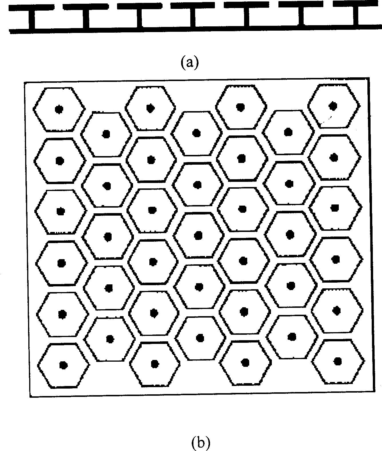
[0032] Example two such as Figure 4 As shown, the silver coil forms a regular hexagon, Figure 4 (a) is a view directly above the second type of high-resistance electromagnetic surface 20, Figure 4 (b) is a schematic structural view of the hexagonal silver coil 21, inside the second type of high-resistance electromagnetic surface 20, there are 7 layers of hexagonal silver coils 21, some air gaps between the hexagonal silver coil 21 and the ceramic matrix Significant shrinkage occurs during calcination, which helps to improve the electrical properties of LC circuits.

[0033] The geometric dimensions of the hexagonal silver coil 21 are as Figure 4 As shown in (a), the hexagonal silver coil 21 is a regular hexagon with a diameter of 2.7mm, and one side is not sealed, and the direction of the unsealed side in the same column is rotated and changed sequentially, and the thickness between the layers of the hexagonal silver coil 21 It is on the order of micron to 1 / 10 millimet...


PUM

PropertyMeasurementUnit
Diameteraaaaaaaaaa
Dielectric constantaaaaaaaaaa

Abstract

The invention provides a solution to high resistance electromagnetic surface and the preparing method. The high resistance electromagnetic surface can prohibit the transmission of electromagnetic wave in some frequency range in the direction of substrate surface, and the ceramic plate device tape-casting printing process can make us flexibly select ceramic material composing mother body to improve and regulate capacitance/inductance property. Based on the existing ripe plate induction device production process, its process flow is as follows: firstly preparing ceramic substrate raw band with a certain thickness by the tape-casting process, printing a layer of flat silver pulp as a bottom electrode on the ceramic substrate raw band by silk-screen; successively preparing a spirally connected silver coil matrix on the bottom electrode by silk-screen and special through hole process, where the bottom ends of these induction coils are connected; making a series of thermal treatment processes on the printed substrate, completing glue arranging and ceramic sintering courses, and obtaining the excellently sintered electromagnetic wave band gap material with a certain mechanical strength and predesigned electrochemical property.

Description

technical field [0001] The invention relates to a high-resistance electromagnetic surface and a preparation method thereof, more specifically, to a periodic multi-layer metal structure high-resistance electromagnetic surface, and to prepare the high-resistance electromagnetic surface on a substrate by using a low-temperature ceramic co-sintering method superficial approach. Background technique [0002] Low-temperature ceramic co-sintering (LTCC) is a method of fabricating microwave devices and circuits, in which (microwave) ceramic powder materials and metal pastes are coated into various patterns and then sintered into different shapes of metal / dielectric at low temperature structure. [0003] Photonic (or electromagnetic) crystals are a new type of material proposed in the 1980s. They form a photonic band gap of a specific frequency and corresponding bandwidth through periodically arranged dielectric or metal structures. In the photonic band gap, electromagnetic waves w...

Claims


Application Information

Patent Timeline
IPC IPC(8): H01Q1/38H01P1/20H01P1/23H01Q21/00
CPCH01P1/2005
Inventor 刘晓晗李博周济资剑
Owner SHANGHAI FANGSHENG INFORMATION TECH
Why Eureka
Try Eureka