Display device and method for manufacturing the same

A technology of a display device and a manufacturing method, which is applied in the directions of lighting devices, semiconductor/solid-state device manufacturing, static indicators, etc., can solve the problems of low-cost production obstacles, inability to become products, and inability to manufacture panels, etc., and achieves the goal of reducing manufacturing costs. Effect

Inactive Publication Date: 2006-06-21
MITSUBISHI ELECTRIC CORP
View PDF1 Cites 0 Cited by
  • Summary
  • Abstract
  • Description
  • Claims
  • Application Information

AI Technical Summary

Problems solved by technology

In this case, even if the superimposed portion different from the above-mentioned crystallinity is used, it can still be clearly and visually recognized on the display, and it cannot be a practical product.
Therefore, in a display device using an actual low-temperature polysilicon thin film transistor, it is impossible to manufacture a panel with the size of the current beam width or more, and it becomes an obstacle to low-cost production that makes full use of the in-plane surface of the glass substrate.

Method used


Image

  • Display device and method for manufacturing the same
  • Display device and method for manufacturing the same
  • Display device and method for manufacturing the same

Examples


Embodiment approach 1

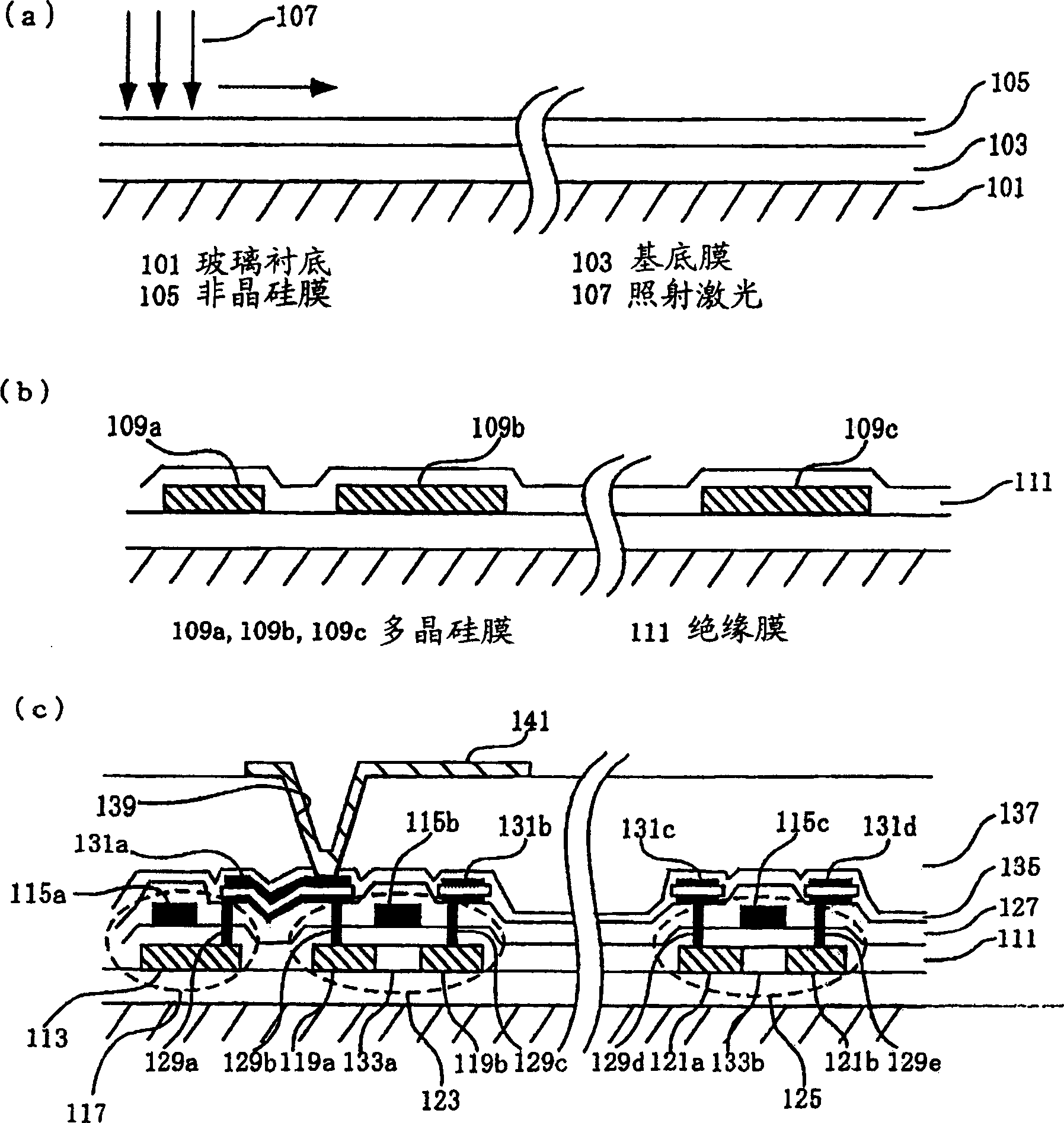
[0034] 1 is a schematic cross-sectional view illustrating a method of manufacturing a thin-film transistor using low-temperature polysilicon and a method of manufacturing a liquid crystal display device using the low-temperature polysilicon according to Embodiment 1 of the present invention. In addition, in the explanatory drawings used in the respective embodiments described below, the same or corresponding parts are denoted by the same reference numerals, and description thereof will be omitted.

[0035] Referring to FIG. 1(a), in the liquid crystal display device in this embodiment mode, firstly, a film with a film thickness of 2500 Å is formed on a glass substrate 101 by, for example, PECVD (Plasma Enhanced Chemical Vapor Deposition: plasma enhanced chemical vapor deposition) method. The base film 103 is composed of left and right silicon oxide films. For the base film 103, a laminated film such as a silicon nitride film, a silicon oxide film, or the like may be used. An ...

Embodiment approach 2

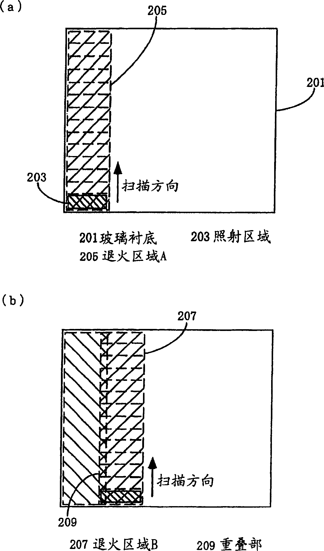
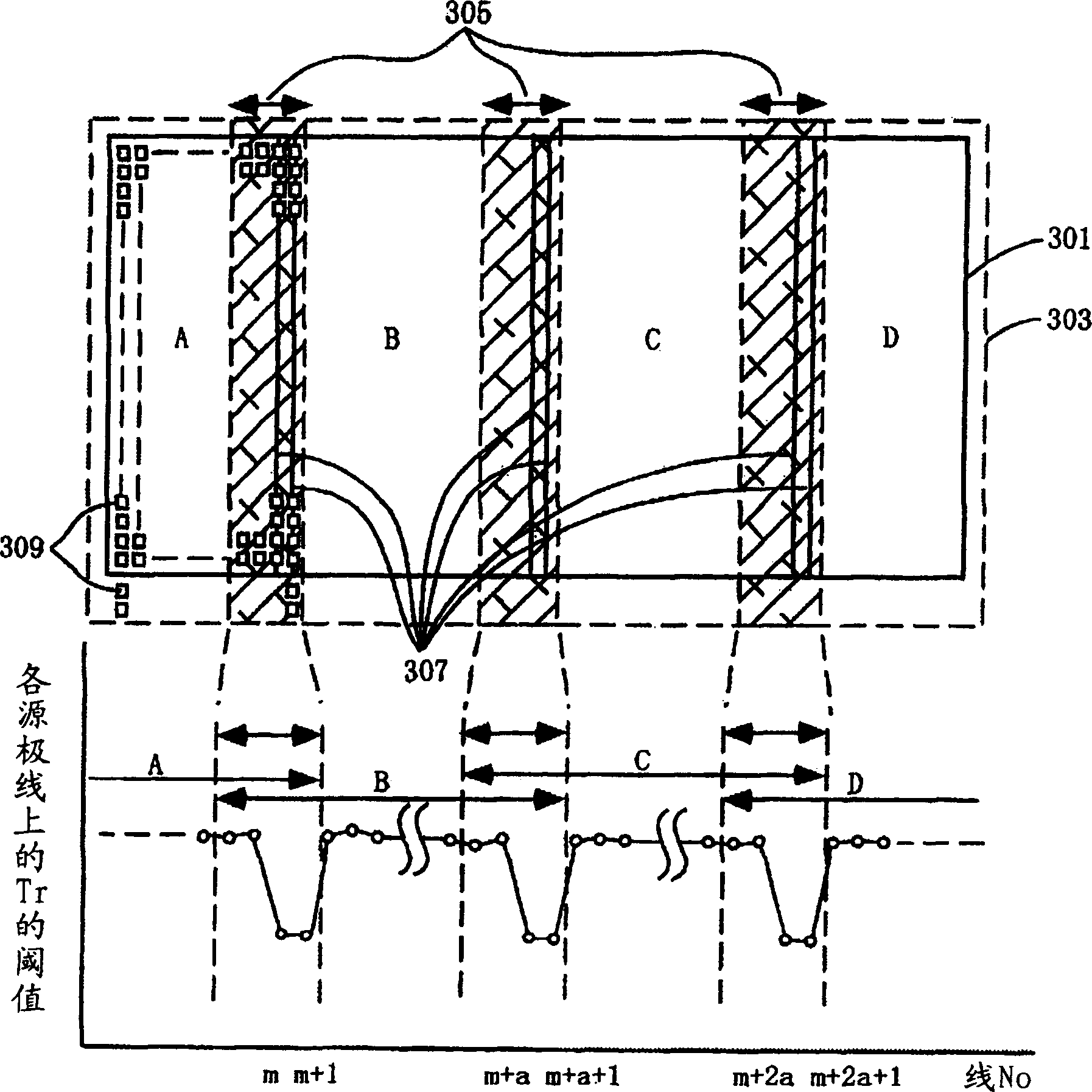
[0056] In Embodiment 1, the panel is arranged so that the overlapping portion of laser light irradiation in laser annealing is parallel to the source lines, and the display unevenness caused by the fluctuation of the threshold value of the thin film transistor on the source line in the overlapping portion is hardly visible. was identified above. On the other hand, in this embodiment, the panel is arranged so that the overlapping portion irradiated with laser light is parallel to the gate lines, so that the display unevenness caused by the fluctuation of the threshold value of the thin film transistor on the gate line in the overlapping portion is hardly visible visually. be identified.


PUM


Abstract

The subject of the present invention is to obtain a display device and a method of manufacturing the same that allow the threshold of thin film transistors to vary within the panel and reduce the manufacturing cost in order to effectively utilize the glass substrate and manufacture a panel having a beam width or more. In order to compensate the difference between the threshold value of the thin film transistor on a specific pixel line and the threshold value of the thin film transistor on other pixel lines, the specific pixel and other pixel lines have different driving circuits, or the driving voltage can be individually adjusted.

Description

technical field [0001] The present invention relates to a display device and a manufacturing method thereof. Background technique [0002] Conventionally, in the development and manufacture of low-temperature polysilicon thin film transistors, a method has been carried out in which amorphous silicon is melted by heat using an excimer laser and then crystallized during cooling to obtain polysilicon in a thin film transistor using polysilicon. Accordingly, since the substrate itself is hardly heated, it is possible to fabricate a thin film transistor on a glass substrate having a low heat-resistant temperature. Furthermore, using this thin film transistor as a driving element, a liquid crystal display device and an organic EL display device are developed and manufactured (for example, refer to Patent Document 1). [0003] [Patent Document 1] Japanese Unexamined Patent Publication No. 2002-341378 (page 4, FIG. 10 ) [0004] As described above, regarding silicon crystallized b...

Claims


Application Information

Patent Timeline
Patent Type & Authority Applications(China)
IPC IPC(8): H01L27/12G02F1/133G02F1/1368H01L21/20H01L21/268H01L21/84H05B33/12
CPCG09G3/20G09G2300/08G09G2310/0267G09G2320/0233G09G2330/028H01L27/1285H01L27/1296G09G3/30
Inventor 久保田健
Owner MITSUBISHI ELECTRIC CORP
Why Eureka
Try Eureka