Planarizing and testing of bga packages

A flat, probe technology, applied in the direction of measuring electricity, measuring devices, measuring electrical variables, etc., can solve problems such as unreliable electrical connections, and achieve the effect of improving electrical connections and improving flatness

Inactive Publication Date: 2006-07-05
CELERITY RES
View PDF0 Cites 8 Cited by
  • Summary
  • Abstract
  • Description
  • Claims
  • Application Information

AI Technical Summary

Problems solved by technology

Such warping results in a non-planar array of term

Method used


Image

  • Planarizing and testing of bga packages
  • Planarizing and testing of bga packages
  • Planarizing and testing of bga packages

Examples


Embodiment Construction

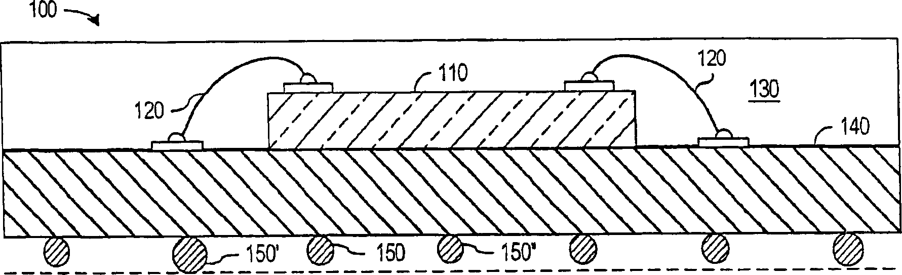
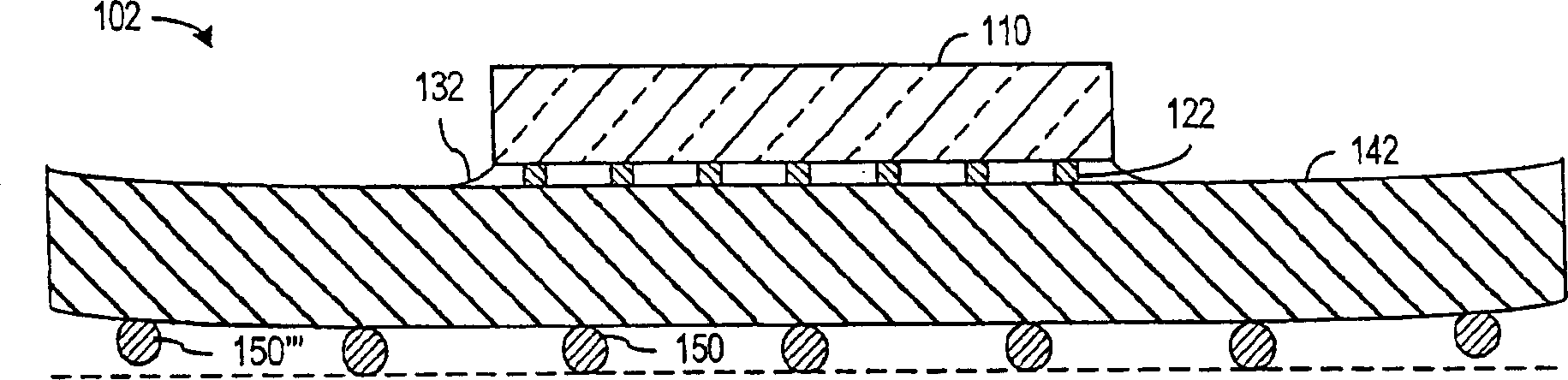
[0017] According to an aspect of the present invention, the test process improves the planarity of external terminals or the like of a semiconductor device package having a BGA. The testing process may employ a contact structure with a probe tip deforming at least the package terminal having the highest height. As a result, the overall variation in package terminal height can be reduced.

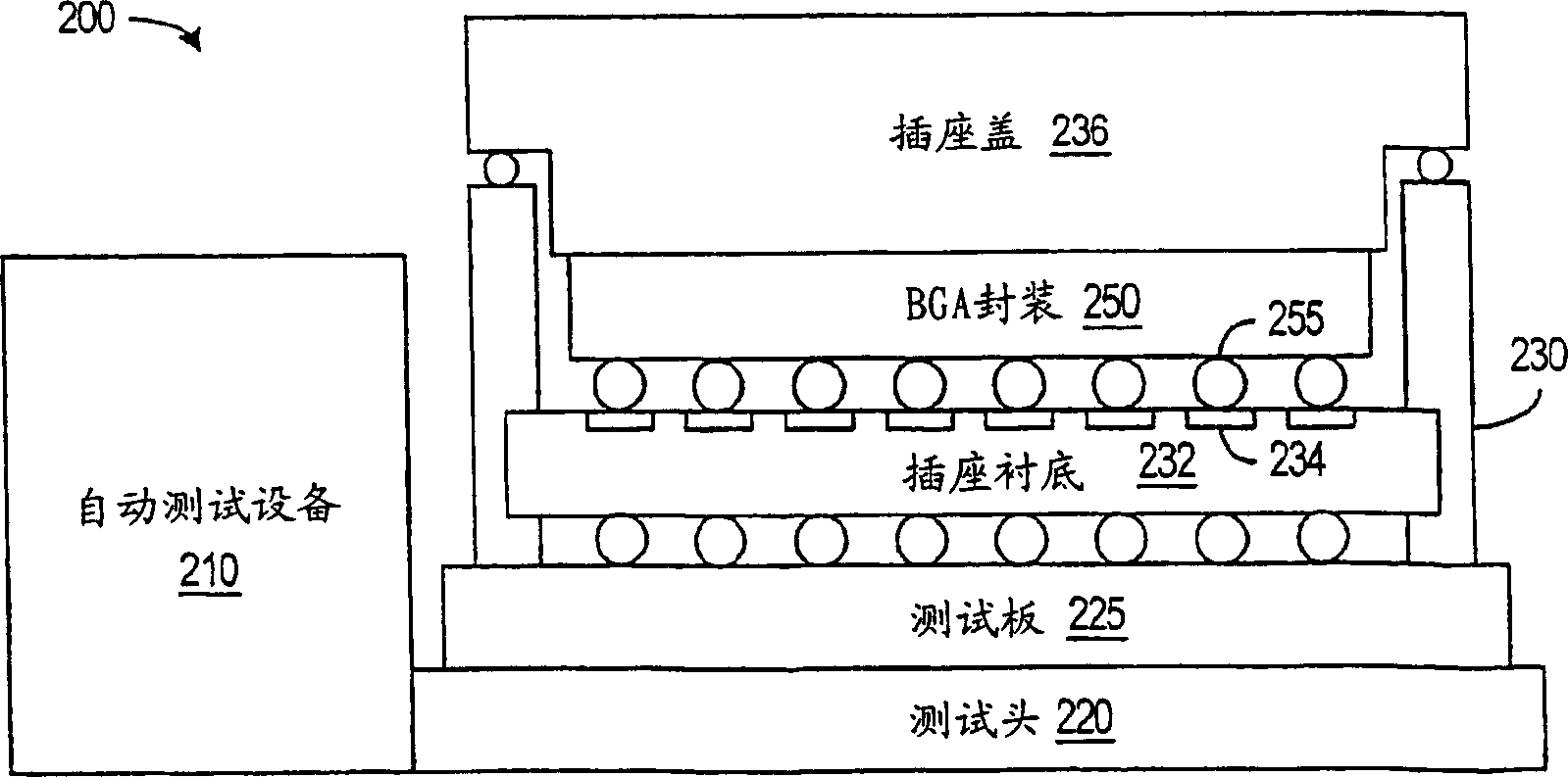
[0018] figure 2 is a block diagram of a test apparatus 200 according to an embodiment of the present invention, which improves the planarity of package terminals. Test equipment 200 includes automatic test equipment (ATE) 210 , test head 220 with test board 225 , socket 230 including socket substrate 232 and socket cover 236 . The testing apparatus 200 electrically tests the package 250 having the external terminals 255 .

[0019] Package 250 may include any type of device or devices including, but not limited to, memory chips, controllers, processors, application specific integrated circ...


PUM


Abstract

The planarity of external terminals or a ball grid array on a device package can be improved through use of test probes that flatten the electrical terminals while forming the electrical contact for package testing. After testing, the package has external terminals with improved planarity that improves the electrical connections formed during assembly of a system containing the package.

Description

Background technique [0001] A ball grid array package (BGA) can provide a packaged integrated circuit device with a high density of terminals. FIG. 1A shows an example of a conventional BGA package 100 including a semiconductor device 110 on an interconnect substrate 140 . Device 110 , which may be any type of semiconductor device, typically has electrical contact pads that are electrically connected to contact pads or traces on interconnect substrate 140 . FIG. 1A shows an example in which wire bonds 120 electrically connect semiconductor device 110 to interconnect substrate 140 , and encapsulant 130 protects and insulates wire bonds 120 . Alternatively, other electrical connection techniques such as flip-chip packaging techniques may provide electrical connections to the interconnect substrate 140 . Interconnect substrate 140 is typically made of an insulator including conductive traces (not shown) that provide electrical signal paths. Contact pads or terminals of device ...

Claims


Application Information

Patent Timeline
IPC IPC(8): G01R31/02G01R1/04G01R1/073G01R1/44
CPCG01R1/0483G01R1/07314G01R1/44
Inventor 马克·L·迪奥里奥
Owner CELERITY RES
Why Eureka
Try Eureka