

Electro-luminescent porous silica material and its preparation method
A technology of electroluminescence and porous silicon, applied in luminescent materials, electroluminescence light sources, electric light sources, etc., can solve the problems of high luminous efficiency, inability to obtain, etc., and achieve the effect of high luminous capacity
- Summary
- Abstract
- Description
- Claims
- Application Information
AI Technical Summary
Problems solved by technology
Method used
Image

Examples
Embodiment 1
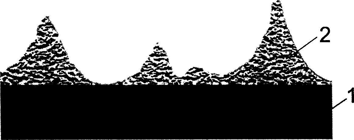
[0013] P-type, boron doped, resistivity 10-12Ωcm, crystal plane index (100), 2mm thick, 1×1cm 2 monocrystalline silicon wafers as raw materials. Clean with deionized water, acetone, and absolute ethanol in sequence, and stick one side with tape after drying. Prepare an etching solution of 3.0 mol / L hydrofluoric acid and 20 ml of 0.01 mol / L silver nitrate, heat to 50° C. under normal pressure, place the silicon wafer above, and keep it warm for 60 minutes. Then soak it in 10% dilute nitric acid for 4 days, take it out and dry it, remove the adhesive tape, place the etched side on the anode of the electrolytic cell, and the cathode is a graphite electrode. Select hydrofluoric acid 6ml, ethanol 9ml, deionized water 12ml (volume ratio) as the etching solution, with a current density of 80mA / cm 2 After etching for 20 minutes, electroluminescent porous silicon with silicon wire structure was obtained. The silicon wires have an average diameter of 235 nm and an average height of 8...
Embodiment 2
[0015] P-type, boron doped, resistivity 10-12Ωcm, crystal plane index (100), 2mm thick, 1×1cm 2 monocrystalline silicon wafers as raw materials. Clean with deionized water, acetone, and absolute ethanol in sequence, and stick one side with tape after drying. Prepare an etching solution of 3.0 mol / L hydrofluoric acid and 20 ml of 0.01 mol / L silver nitrate, heat to 60° C. under normal pressure, place the silicon wafer above, and keep it warm for 60 minutes. Then soak it in 10% dilute nitric acid for 4 days, take it out and dry it, remove the adhesive tape, place the etched side on the anode of the electrolytic cell, and the cathode is a graphite electrode. Select 1ml of hydrofluoric acid, 10ml of ethanol, and 10ml of deionized water (volume ratio) as the etching solution, and sequentially use a current density of 30mA / cm 2 Etching for 30 minutes and 20mA / cm 2 After etching for 30 minutes, electroluminescent porous silicon with a silicon line structure was obtained.
Embodiment 3
[0017] P-type, boron doped, resistivity 10-12Ωcm, crystal plane index (110), 2mm thick, 1×1cm 2 monocrystalline silicon wafers as raw materials. Clean with deionized water, acetone, and absolute ethanol in sequence, and stick one side with tape after drying. Prepare an etching solution of 1.5 mol / L hydrofluoric acid and 20 ml of 0.01 mol / L silver nitrate, heat to 40° C. under normal pressure, place the silicon wafer above, and keep it warm for 60 minutes. Then soak it in 10% dilute nitric acid for 4 days, take it out and dry it, remove the adhesive tape, place the etched side on the anode of the electrolytic cell, and the cathode is a graphite electrode. Select 6ml of hydrofluoric acid, 9ml of ethanol, and 12ml of deionized water (volume ratio) as the etching solution, and sequentially use a current density of 30mA / cm 2 Etching for 30 minutes and 20mA / cm 2 After etching for 30 minutes, electroluminescent porous silicon with a silicon line structure was obtained.
PUM
| Property | Measurement | Unit |
|---|---|---|
| Resistivity | aaaaa | aaaaa |
| Average height | aaaaa | aaaaa |
| Facet index | aaaaa | aaaaa |
Abstract
Description
Claims
Application Information