Three-dimensional integrated circuit structure and method of making same

A technology for gate electrodes and electrical devices, applied in circuits, semiconductor/solid-state device manufacturing, electrical components, etc., can solve problems that have not been widely used

Inactive Publication Date: 2006-07-26
飞上公司
View PDF14 Cites 15 Cited by
  • Summary
  • Abstract
  • Description
  • Claims
  • Application Information

AI Technical Summary

Problems solved by technology

[0007] However, the above-mentioned laser recrystallization and epitaxy processes have disadvantages, such as the need for high-temperature operation, which contradicts the low-temperature processing required by many semiconductor devices; in addition, the single crystal semiconductor layer formed in this way also has many defects, so these method is not widely used

Method used


Image

  • Three-dimensional integrated circuit structure and method of making same
  • Three-dimensional integrated circuit structure and method of making same
  • Three-dimensional integrated circuit structure and method of making same

Examples


Embodiment Construction

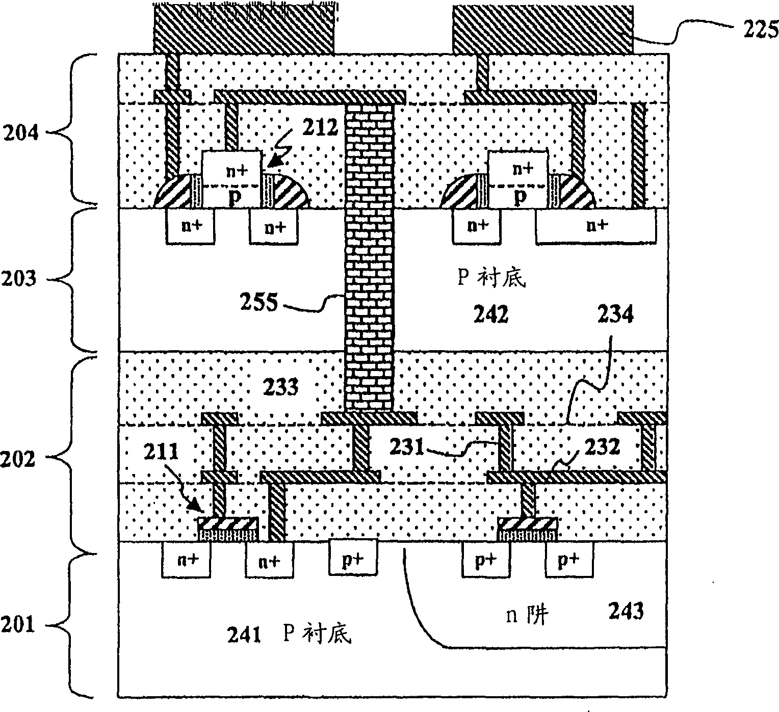
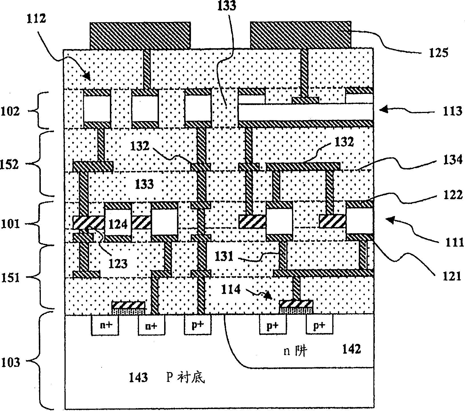
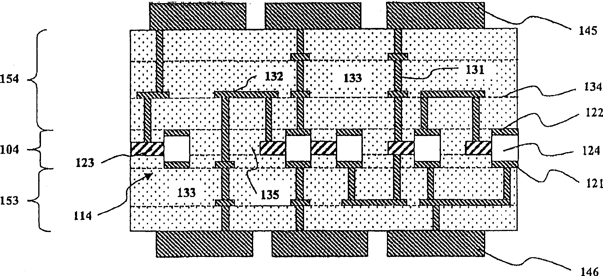
[0065] exist figure 2 A 3-D IC according to the present invention is shown in . An embodiment of the present invention provides a device integration technology.

[0066] "One embodiment", "an embodiment" or similar expressions referred to herein mean that at least one embodiment of the present invention includes specific features, structures, operations or characteristics described with reference to the embodiment. Thus, appearances of such phrases or expressions are not necessarily all referring to the same embodiment. Furthermore, the various specific features, structures, operations or characteristics may be combined in any suitable manner in one or more embodiments.

[0067] the term

[0068] "ASIC" means Application Specific Integrated Circuit. "SoC" refers to a system on a chip (System on a Chip), and "SoCs" is the plural of SoC. A SoC can be an ASIC, but it doesn't have to be. An ASIC can be a SoC, but it doesn't have to be.

[0069] The expression "back bias" as...


PUM


Abstract

A plurality of semiconductor devices (111,122,113) with vertical orientation are separated physically and mutually and are not arranged on the same semiconductor main body or a semiconductor substrate. The semiconductor devices (111,112,113) can be arranged on a substrate (103) produced separately and are used as a thin layer which contains a plurality of doping semiconductor areas; the semiconductor devices are jointed and then are etched to generate each doping superposition structure; alternatively, the semiconductor devices (111,112,113) can be produced before the devices are jointed with the substrate (103). The doping superposition structure can form the basis of diode, capacitor or transistor device; wherein, an auxiliary layer which can be laminated can include an interconnection line (132).

Description

technical field [0001] The present invention relates generally to three-dimensional integrated circuit (IC) structures and methods of fabrication thereof, and more particularly to the integration of semiconductor substrates with thin add-on semiconductors in which various active and / or passive devices have been fabricated. Layers are combined. Background technique [0002] As shown in Figure 1, prior art 3-D ICs may be referred to as "hybrid ICs". Conventional hybrid IC implementation methods typically include the following steps: providing a first IC that includes a base semiconductor substrate 201 and a dielectric layer 202; providing a second IC that also includes a base semiconductor substrate 203 and a dielectric layer 204; stacking and bonding these IC or a separate chip; and implementing deep vias 255 through the semiconductor substrate as shown in US Patent 6,600,173, or providing micro bumps as shown in US Patent 6,355,501. [0003] Continuing to refer to FIG. 1 ,...

Claims


Application Information

Patent Timeline
Patent Type & Authority Applications(China)
IPC IPC(8): H01L21/30H01L21/46H01L21/301H01L21/334
CPCH01L2924/0002H01L2924/00B82Y30/00H01L21/18
Inventor 李相润
Owner 飞上公司
Why Eureka
Try Eureka