Semiconductor element and making method

A manufacturing method and semiconductor technology, applied in semiconductor/solid-state device manufacturing, semiconductor devices, electrical components, etc., can solve problems such as read-only memory high-voltage components cannot be integrated, and achieve the effect of shortening the manufacturing process and reducing manufacturing costs

Active Publication Date: 2006-08-09
UNITED MICROELECTRONICS CORP
View PDF0 Cites 1 Cited by
  • Summary
  • Abstract
  • Description
  • Claims
  • Application Information

AI Technical Summary

Problems solved by technology

[0005] Another object of the present invention is to provide a method for manufacturing a semiconductor element. In addition to solving the problem that the existing erasable programmable read-only memory cannot be integrated with high-voltage elements, this method can also integrate low-voltage elements or other Semiconductor components are integrated with the first two processes to improve manufacturing efficiency

Method used


Image

  • Semiconductor element and making method
  • Semiconductor element and making method
  • Semiconductor element and making method

Examples


Embodiment Construction

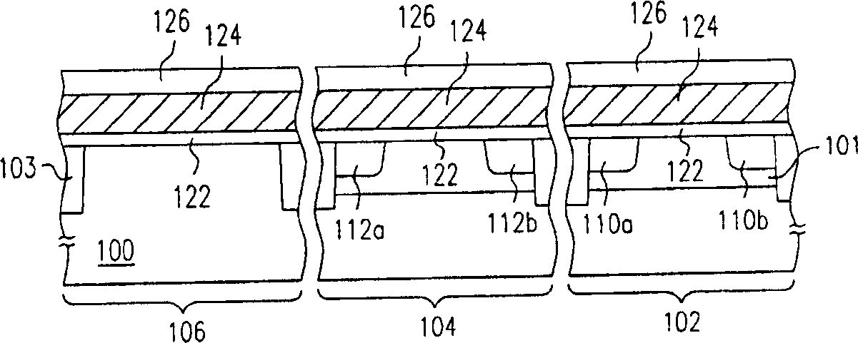
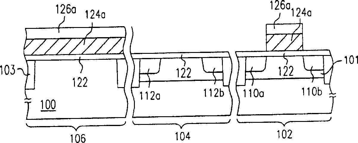
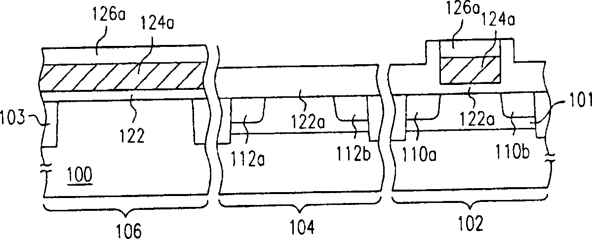
[0048] Figure 1A to Figure 1G is a cross-sectional view illustrating a manufacturing process of a semiconductor device according to a preferred embodiment of the present invention.

[0049] Please refer to Figure 1A, the manufacturing method of the semiconductor device of the present invention firstly provides a substrate 100 , the substrate 100 has a memory cell area 102 , a high voltage circuit area 104 and a low voltage circuit area 106 . The material of the substrate 100 is, for example, a silicon substrate, and the substrate 100 is, for example, a P-type silicon substrate or an N-type silicon substrate according to the type of semiconductor device to be formed. Afterwards, an isolation structure 103 is formed on the substrate 100 to define a plurality of active device regions (not shown), and isolate the memory cell region 102 , the high voltage circuit region 104 , and the low voltage circuit region 106 . The isolation structures 103 are, for example, field oxide laye...


PUM


Abstract

The method includes following steps: providing a substrate with storage unit zone and high voltage circuit zone; forming first, second source poles / drain poles zones on the two pieces of zone in the substrate; forming oxidizing layer, first conductive layer and topping layer in sequence on the substrate; defining floating grid on the storage unit zone, and removing out the topping layer and the first conductive layer from the high voltage circuit zone; thickening exposed the oxidizing layer; removing out the topping layer, and forming barrier layer on the exposed surface of floating grid; forming second conductive layer, defining out grid pole in the high voltage circuit zone, and defining out control grid pole in storage unit zone. Combining procedure for preparing storage unit and high voltage components, the method does not need to increase number of using photoresist so as to shorten fabricating flow and lowering fabricating cost.

Description

technical field [0001] The invention relates to a manufacturing method of an integrated circuit, in particular to a semiconductor element and a manufacturing method thereof. Background technique [0002] Non-volatile memory (Non-Volatile Memory) due to its circuit design, the stored memory or data will not disappear due to power supply interruption, and the data can be stored, read and cleared multiple times, and its It has the advantages of small size, fast access speed and low power consumption, and there is considerable demand for it in the market. However, the current non-volatile memory integrated with the high-voltage device process is a single-layer polysilicon one-time programmable device. This kind of single-layer polysilicon one-time programmable device is commonly used in the general industry because its structure is similar to that of general high-voltage devices, and it is relatively easy in process integration. However, due to its low tolerance, the single-la...

Claims


Application Information

Patent Timeline
Patent Type & Authority Applications(China)
IPC IPC(8): H01L21/8239H01L27/105
Inventor 李文芳徐尉伦林育贤
Owner UNITED MICROELECTRONICS CORP
Why Eureka
Try Eureka