PLL frequency synthesizer

A frequency synthesizer and frequency divider technology, applied in the direction of automatic power control, electrical components, etc., can solve the problems of increased circuit area, increased product size of PLL frequency synthesizers, and increased prices, and achieves simple structure, high The effect of performance, low price

Inactive Publication Date: 2006-08-16
PANASONIC CORP
View PDF1 Cites 5 Cited by
  • Summary
  • Abstract
  • Description
  • Claims
  • Application Information

AI Technical Summary

Problems solved by technology

[0016] However, the above-mentioned conventional technology has the following problems: since the A/D converter, DSP, and D/A converter are required, the price is increased, the circuit area is greatly incre...

Method used


Image

  • PLL frequency synthesizer
  • PLL frequency synthesizer
  • PLL frequency synthesizer

Examples


no. 1 Embodiment approach

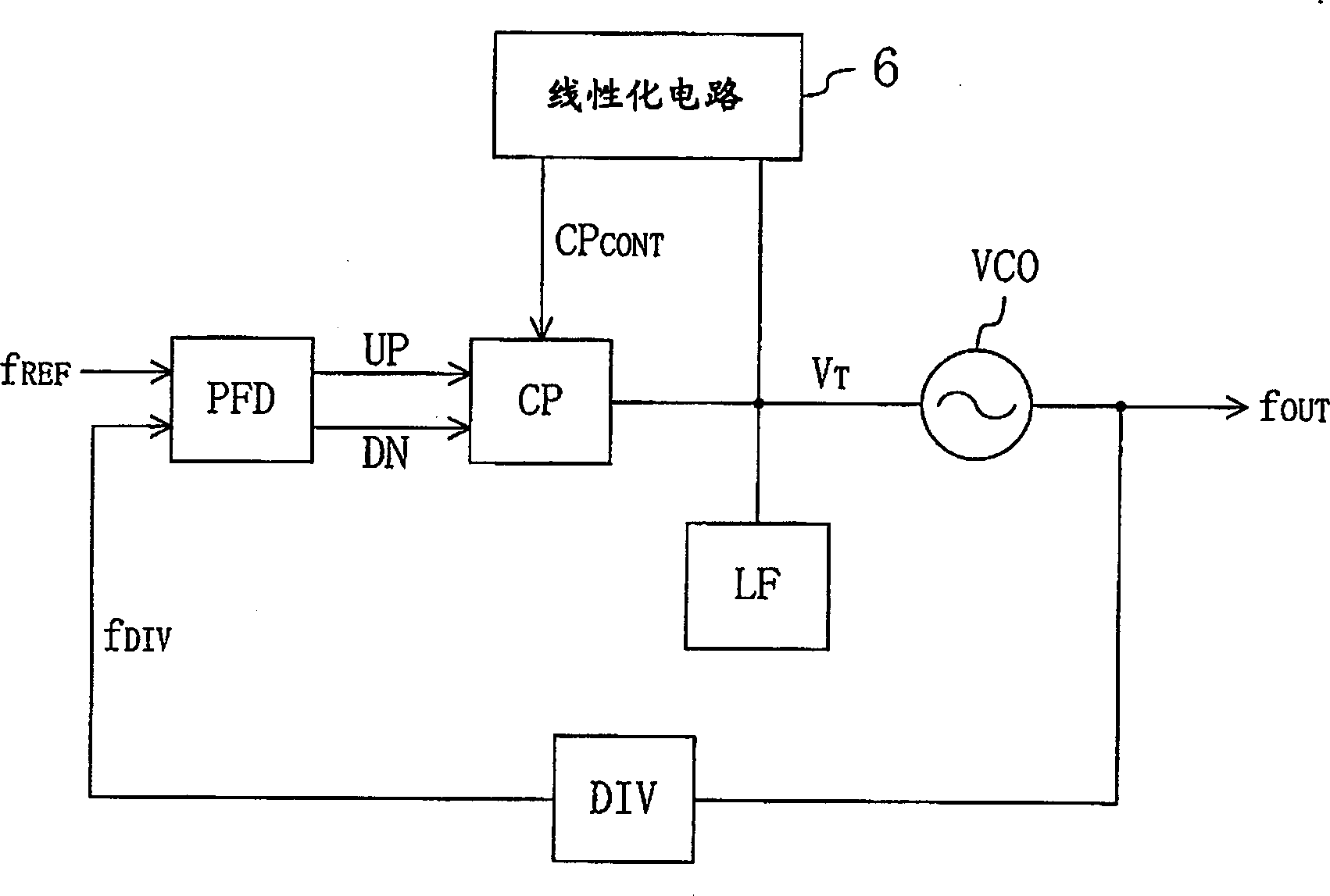
[0048] figure 1 It is a diagram showing the configuration of the PLL frequency synthesizer according to the first embodiment of the present invention.

[0049] In the figure, the PLL frequency synthesizer has a voltage-controlled oscillator VCO, a programmable frequency divider DIV, a phase comparator PFD, a charge pump circuit CP, and a loop filter LF.

[0050] The voltage-controlled oscillator VCO mentioned above controls the signal V according to the oscillation frequency T The voltage changes the oscillation frequency. The above frequency divider DIV compares the oscillation frequency f from the voltage controlled oscillator VCO with the frequency division ratio corresponding to the channel selection signal input from the outside. OUT Carry out frequency division. The above-mentioned phase comparator PFD detects the output signal f from the above-mentioned division frequency DIV DIV with an externally input reference signal f REF The phase difference between them out...

no. 2 Embodiment approach

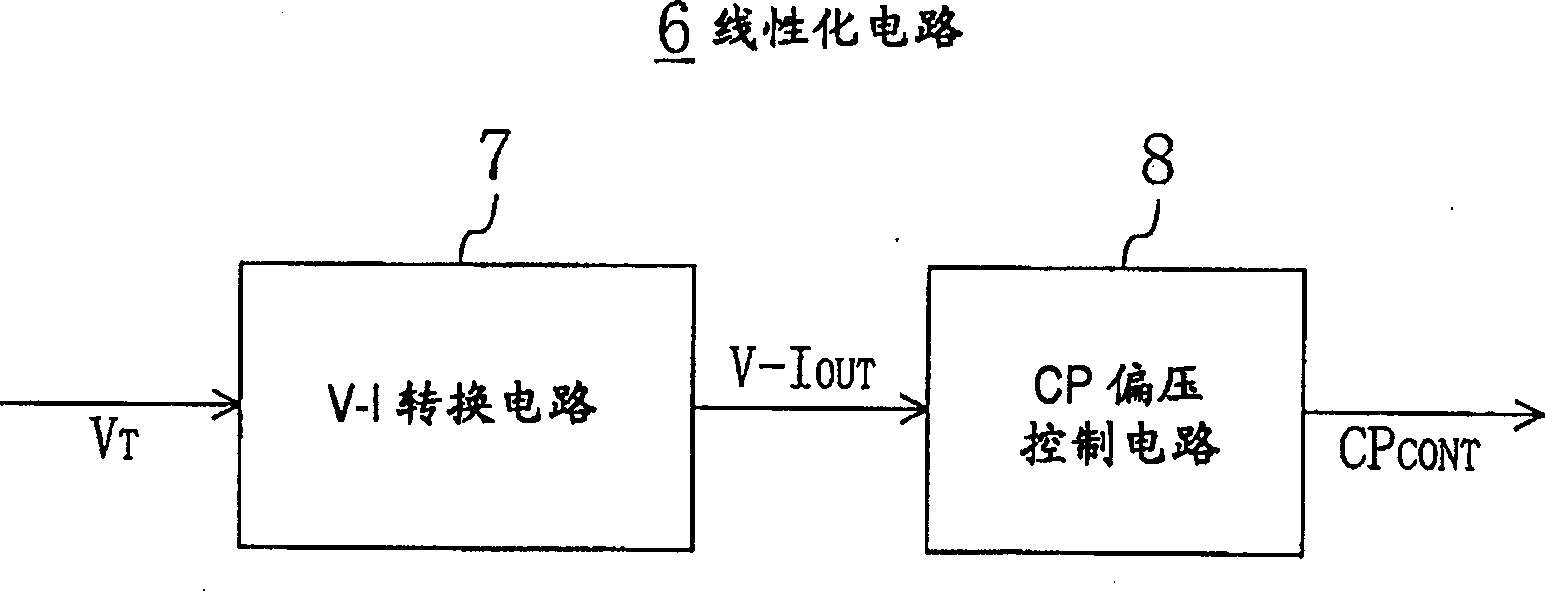
[0058] Next, a second embodiment of the present invention will be described. This embodiment is a modification of the linearization circuit 6 shown in the above-mentioned first embodiment.

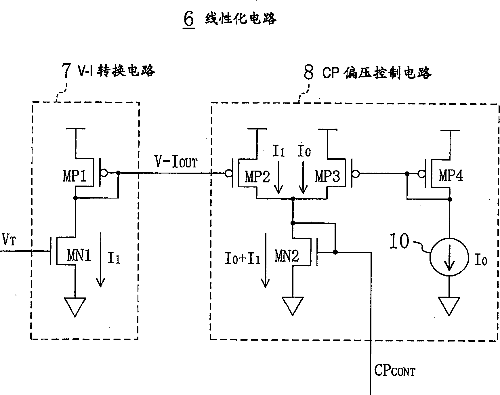
[0059] Right now, Figure 5 In the shown linearization circuit 6', two series circuits of P-type and N-type transistors MP1A and MN1A and other series circuits of P-type and N-type transistors MP1B and MN1B are arranged in the V-I conversion circuit 7'. circuit, the oscillating frequency signal V from the loop filter LF above T They are respectively input to the gates of the two N-type transistors MN1A and MN1B mentioned above. Therefore, with image 3 The shown V-I conversion circuit 7 similarly flows through the current I of the two N-type transistors MN1A and MN1B of each series circuit respectively. 1A , I 1B , according to the oscillation frequency signal V received by the gate of the respective transistor T potential changes. Moreover, in the CP bias control circuit 8', there ...

no. 3 Embodiment approach

[0063] Next, a third embodiment of the present invention will be described. This embodiment is a modification of the linearization circuit 6 shown in the above-mentioned first embodiment.

[0064] Right now, Figure 7 The shown linearization circuit 6 ", in the V-I conversion circuit 7 ", receives the oscillation frequency control signal V at the gate T An N-type transistor MN3 is disposed between the source of the N-type transistor MN1 and the ground. An operational amplifier 12 is connected to the gate of the N-type transistor MN3 , and the source voltage of the N-type transistor MN1 and a bias voltage generated by the bias voltage generating circuit 11 are input to the operational amplifier 12 . The operational amplifier 12 controls the N-type transistor MN3 such that the source voltage of the N-type transistor MN1 matches the bias voltage generated by the bias voltage generating circuit 11 . in addition, Figure 7 shown in the CP bias control circuit 8, with figure 1...


PUM


Abstract

In a PLL frequency synthesizer, a linearization circuit (6) is provided which receives an oscillation frequency control signal (VT) from a loop filter (LF). The linearization circuit (6) outputs, in accordance with the potential level of the oscillation frequency control signal (VT), a charge pump current control signal (CPCONT) that exhibits the higher value, the higher the potential level. The charge pump (CP) receives the charge pump current control signal (CPCONT) to cause a current in accordance with the value of the received charge pump current control signal (CPCONT) to flow in or flow out. Thus, a simple circuit arrangement can be used to adjust and maintain constant the loop gain characteristic of the PLL frequency synthesizer. Accordingly, even when a variable capacitance element included in the a voltage controlled oscillator has a nonlinear characteristic for the potential of the input oscillation frequency control signal, the loop gain of the PLL frequency synthesizer having this voltage controlled oscillator can be adjusted and maintained constant.

Description

technical field [0001] The present invention relates to a PLL frequency synthesizer used in a semiconductor integrated circuit in the wireless communication field for transmitting / receiving local signals required for radio waves, and more particularly to improvement of the characteristics of the PLL frequency synthesizer. Background technique [0002] The structure of the conventional PLL frequency synthesizer is expressed as Figure 11 . [0003] Figure 11 The conventional PLL frequency synthesizer shown has a voltage-controlled oscillator VCO, a programmable frequency divider DIV, a phase comparator PFD, a charge pump circuit CP, and a loop filter LF. [0004] The voltage-controlled oscillator VCO mentioned above controls the signal V according to the oscillation frequency T (described later) changes the oscillation frequency. The frequency divider DIV divides the oscillation frequency from the voltage controlled oscillator VCO by a frequency division ratio correspondin...

Claims


Application Information

Patent Timeline
IPC IPC(8): H03L7/093
CPCH03L7/093H03L7/0898H03L7/18
Inventor 泽田昭弘
Owner PANASONIC CORP
Why Eureka
Try Eureka