Mems device and manufacturing method of mems device
A manufacturing method and component technology, applied in the field of MEMS components, can solve the problems of damage to wiring 105, poor humidity resistance, and reduced reliability of MEMS components 100, and achieve the effects of improved reliability and good humidity resistance
- Summary
- Abstract
- Description
- Claims
- Application Information
AI Technical Summary
Problems solved by technology
Method used
Image

Examples
no. 1 approach
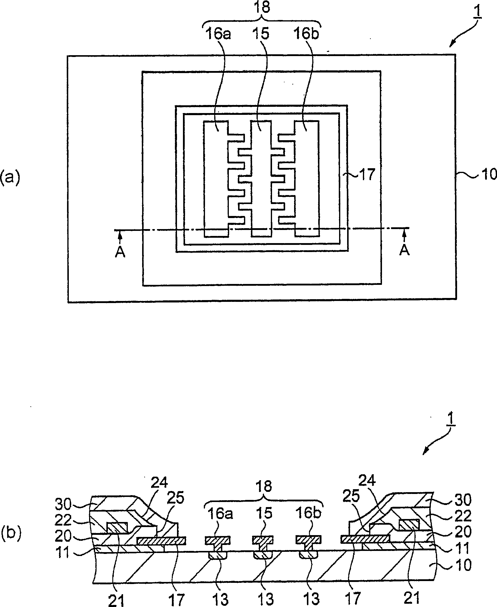
[0048] figure 1 It is a schematic configuration diagram showing an embodiment of a MEMS resonator as a MEMS element of the present invention. in, figure 1 (a) is a top view of the MEMS element, figure 1 (b) is a cross-sectional view along the line A-A of (a) in this figure.
[0049] exist figure 1 In the MEMS element 1, a structure 18 consisting of a movable electrode 15 and fixed electrodes 16a, 16b made of polysilicon is formed on a semiconductor substrate 10 made of silicon. An n-type lower electrode 13 is formed on the semiconductor substrate 10 to be electrically connected to the structure 18 . In addition, an insulating film 11 which is a thermally oxidized film formed on the semiconductor substrate 10 is formed on a peripheral portion facing the structure 18, and an interlayer insulating film 20, wiring 21, and interlayer insulating film 22 are sequentially stacked thereon. . The wiring 21 is made of Al, Cu, or the like, and is connected to the lower electrode...
no. 2 approach
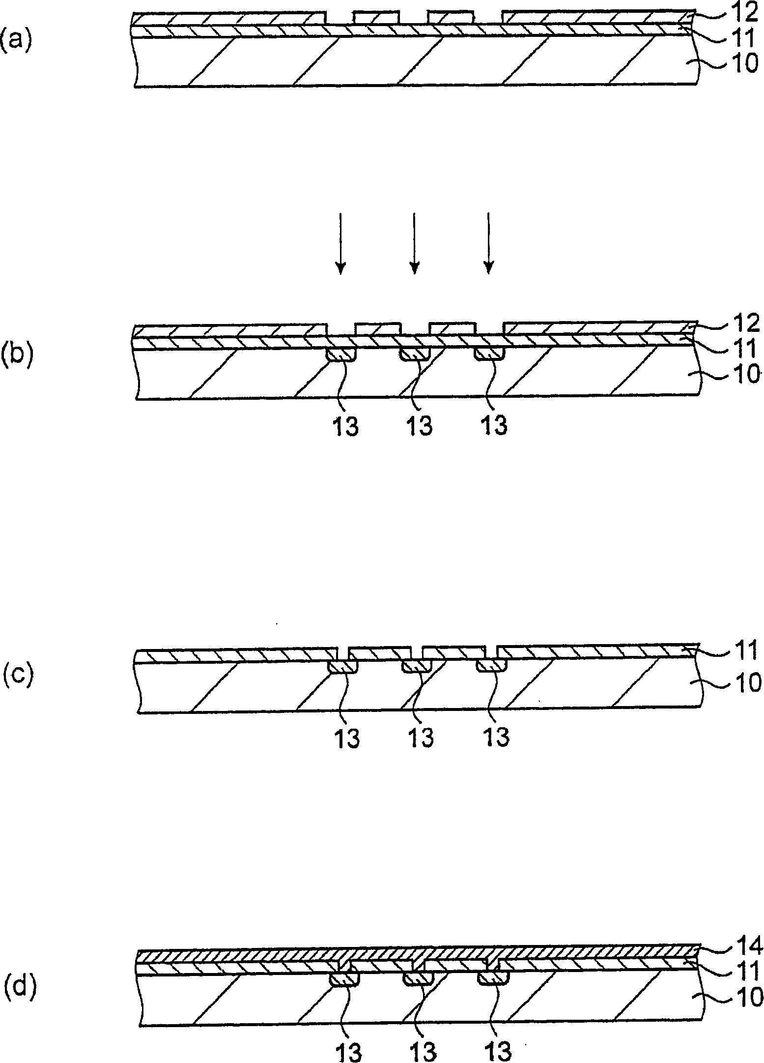
[0056] Next, a method of manufacturing the MEMS element 1 will be described. For the manufacture of this MEMS component, a semiconductor CMOS process is used.
[0057] figure 2 , image 3 , Figure 4 It is a schematic cross-sectional view showing the manufacturing process of the MEMS element 1 .
[0058] First, in figure 2 In (a), a thermal oxide film (SiO 2 film), that is, an insulating film 11, on which a photoresist is applied to form a photoresist film 12. Then, the photoresist film 12 is patterned into a predetermined shape. Thereafter, if figure 2 As shown in (b), P ions are implanted from above the patterned semiconductor substrate 10 to form an n-type lower electrode 13 on the semiconductor substrate 10 . Next, the photoresist film 12 is removed, a photoresist is applied again, and patterning is performed to remove a part of the insulating film 11 above the lower electrode 13 . Then, if figure 2 As shown in (c), part of the insulating film 11 is etched up...
no. 3 approach
[0072] Figure 6 It is a schematic configuration diagram showing another embodiment of a MEMS resonator as a MEMS element of the present invention. Figure 6 (a) is a top view of the MEMS element, Figure 6 (b) is a sectional view along the line B-B of (a) in this figure.
[0073] exist Figure 6 In the MEMS element 2, a structure body 50 composed of an upper structure body 49 and a lower structure body 44 is formed on a semiconductor substrate 40 made of silicon through a nitride film 41. The upper structure body 49 and the lower structure body 44 are made of polysilicon constitute. The upper structure 49 and the lower structure 44 each function as an electrode, and are arranged to overlap a part of the upper structure 49 in the thickness direction with a constant interval above the lower structure 44 .
[0074] In addition, in the peripheral portion facing the structure 50, interlayer insulating films 45, 51, wiring lines 52, 53, and interlayer insulating film 54 are seq...
PUM
 Abstract
Description
Claims
Application Information
PatSnap Eureka turns technology decisions into work you can execute. Powered by our Innovation Knowledge Graph, it runs expert workflows across engineering, life sciences, materials and intellectual property. Get your review-ready output in minutes.


