Microfluidic chip with sampling probe and preparation method thereof

A microfluidic chip and probe technology, applied in the direction of analyzing materials, instruments, etc., can solve the problems of large tip section, low success rate, troublesome and other problems, and achieve the effect of simple and easy operation, convenient sampling operation and fast processing speed.

Inactive Publication Date: 2006-09-27
ZHEJIANG UNIV
View PDF0 Cites 8 Cited by
  • Summary
  • Abstract
  • Description
  • Claims
  • Application Information

AI Technical Summary

Problems solved by technology

[0003] At present, most of the microfluidic chip analysis systems adopt the method of fixed liquid storage pools, that is, several liquid storage pools are vertically fixed at the entrance and exit of the chip channel, and the sample and reagent solutions are added to each liquid storage pool before analysis. , the biggest disadvantage of this analysis system is: when replacing the solution in the liquid pool, the operation steps are cumbersome, laborious, and inefficient, and the time for changing the liquid is far longer than the analysis time, which seriously affects the analysis speed of the entire system; Most fluidic chip analysis systems can only use simple detection methods such as fluorescence, and it is difficult to directly combine with mass spectrometry and other detectors
Although this kind of capillary probe solves the interface problem between the chip and the external sample or detection system, the technical difficulty of this kind of connection is high, the success rate is low, and there is a certain interface dead volume between the capillary and the chip channel, which is harmful to the system. Analytical performance will have a large impact
Wang et al. (Chen G, Wang J. Fast and Simple Introduction for Capillary Electrophoresis Microsystems, Analyst, 2004, 129: 507) proposed a simple and rapid sample introduction method for microfluidic chip capillary electrophoresis analysis, which is characterized by : Use a diamond saw to directly process the sampling probe in situ at the end of the chip channel, but this method can only be used for cutting on both sides of the chip channel, the probe is square, and its tip cross-section is large, so the sampling operation is more difficult

Method used


Image

  • Microfluidic chip with sampling probe and preparation method thereof
  • Microfluidic chip with sampling probe and preparation method thereof
  • Microfluidic chip with sampling probe and preparation method thereof

Examples


Embodiment 1

[0027] Glass integrated probe microfluidic chip, the steps and methods of submillimeter probes are:

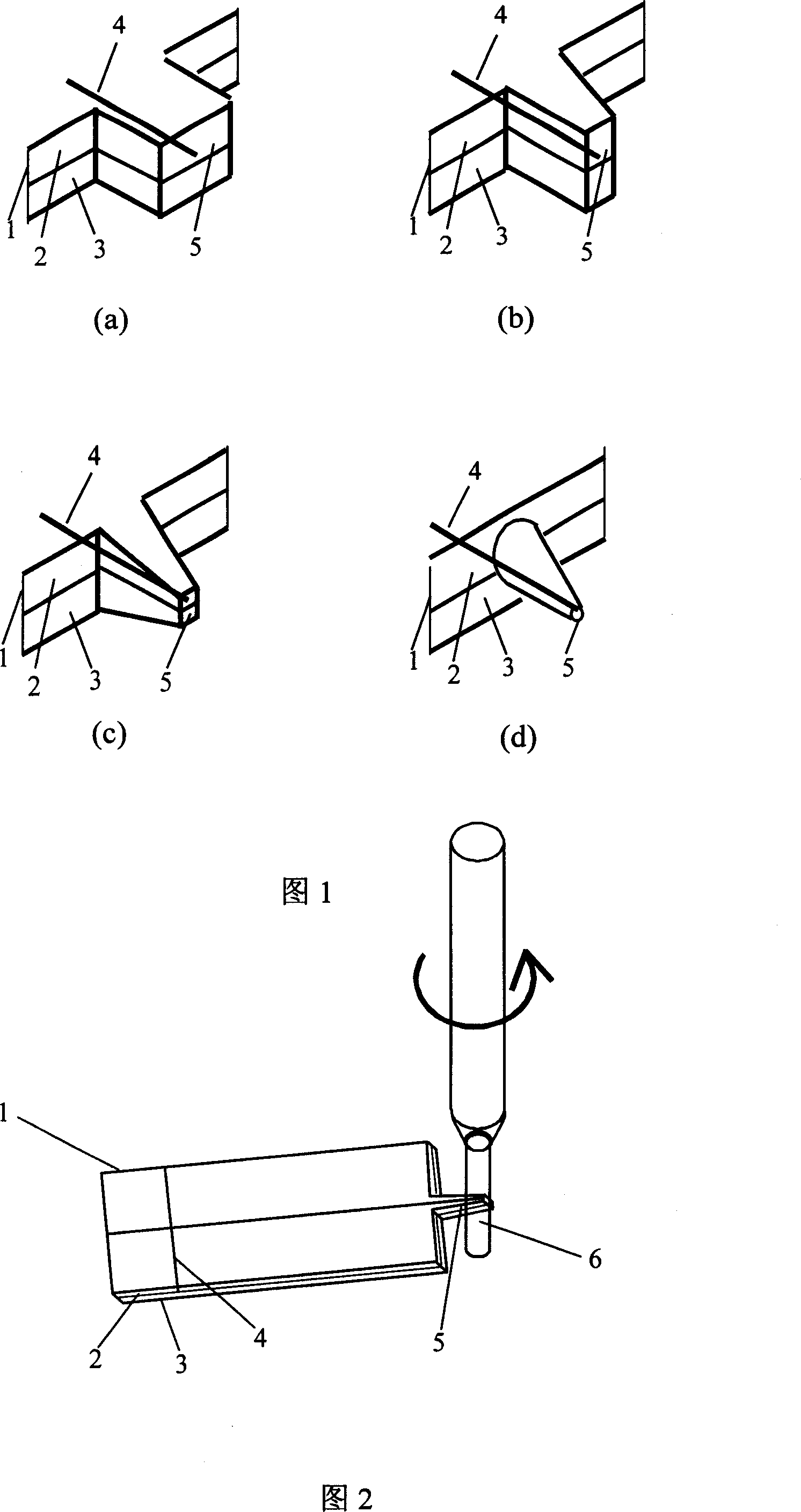
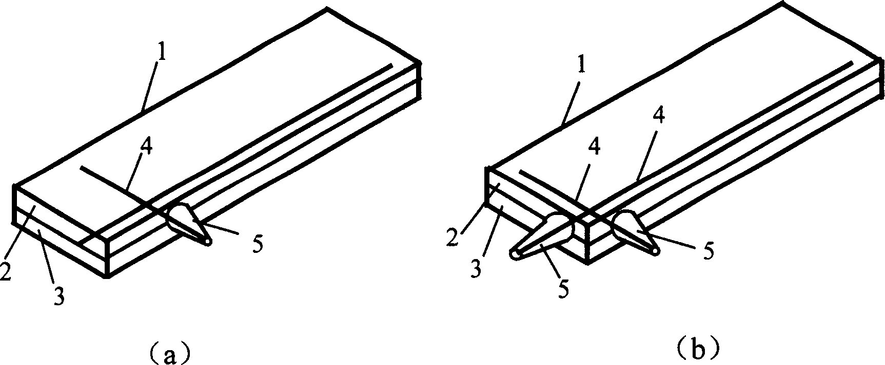
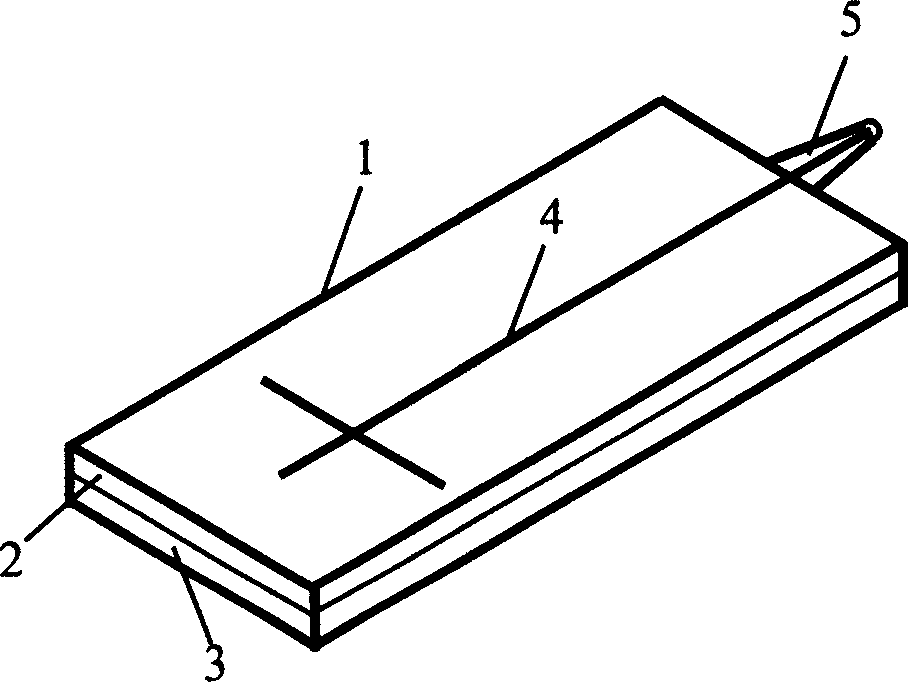
[0028] As shown in FIG. 1 , the microfluidic substrate 1 is composed of a glass upper sheet 2 and a glass lower sheet 3 etched with microchannels 4 , and the two sheets are sealed by high-temperature bonding. The channel depth ranges from 1 to 100 microns, and the width ranges from 1 to 500 microns. Before processing the probe, apply a small amount of epoxy resin glue liquid on the entrance of the end of the substrate channel 4. After curing, an epoxy resin "protection plug" about 0.5-1 mm long is formed to pre-protect the entrance of the channel to prevent When the probe is processed, glass slag enters the channel and causes channel blockage. The specific processing process of the glass microfluidic chip integrated probe is as shown in Figure 1: use a glass knife to cut the end of the substrate channel 4 to form a rectangular probe 5 prototype with a width of 2 mm x 3.4 mm h...

Embodiment 2

[0031] Glass-integrated probe-type microfluidic chip, the steps and methods of micron-scale probes are:

[0032] As shown in FIG. 1 , the microfluidic substrate 1 is composed of a glass upper sheet 2 and a glass lower sheet 3 etched with microchannels 4 , and the two sheets are sealed by high-temperature bonding. The channel depth ranges from 1 to 50 microns, and the width ranges from 1 to 50 microns. Before processing the probe, a small amount of epoxy resin glue liquid is applied to the entrance of the end of the substrate channel 4, and after curing, an epoxy resin "protection plug" about 0.5-1 mm long is formed to pre-protect the channel entrance. The process of drilling and grinding the glass microfluidic chip integrated probe with the grinding head is as shown in Figure 1: use a glass knife to cut the end of the substrate channel 4 to form a rectangular probe with a width of 2 mm x 3.4 mm high x 1-30 mm long. The prototype of needle 5 (as shown in Figure 1(a)). A cylin...


PUM

PropertyMeasurementUnit
diameteraaaaaaaaaa
diameteraaaaaaaaaa
diameteraaaaaaaaaa

Abstract

This invention relates to a microfluidic chip with sampling probe and preparation method thereof, which comprises a substrate with an upper and lower piece, a micro channel, and one or more conical sample probe with pinpoint size in 5um-2mm on micro-channel back input on side wall of the substrate. This invention is simple and practical.

Description

technical field [0001] The invention relates to the field of microfluidic chip analysis, in particular to an integrated probe microfluidic chip and a preparation method thereof. Background technique [0002] Since the rise of microfluidic chip analysis technology in the early 1990s, it has become one of the research hotspots in the field of analytical chemistry due to its characteristics of miniaturization, rapidity, high efficiency and high throughput. The structure of the microfluidic analysis chip is generally two pieces of flat materials, one of which is engraved with a network of fine channels through micromachining technology, and the corresponding channel inlet and outlet are processed on any piece, and then the two pieces of flat plates are sealed together to form a closed channel. chip. [0003] At present, most of the microfluidic chip analysis systems adopt the method of fixed liquid storage pools, that is, several liquid storage pools are vertically fixed at the...

Claims


Application Information

Patent Timeline
Patent Type & Authority Applications(China)
IPC IPC(8): G01N35/00
Inventor 何巧红方群
Owner ZHEJIANG UNIV
Why Eureka
Try Eureka