Method for manufacturing nanometer paster

A manufacturing method and nanotechnology, applied in nanotechnology, nanotechnology, photoengraving process of patterned surface, etc., can solve the problem of unable to meet the needs of the industry, unable to meet the needs of mass production and low cost, unable to meet the needs of mass production, etc. question

Inactive Publication Date: 2006-10-04
CONTREL TECH CO LTD
View PDF1 Cites 3 Cited by
  • Summary
  • Abstract
  • Description
  • Claims
  • Application Information

AI Technical Summary

Problems solved by technology

[0003] Among the currently known technologies, there is a scanning electron beam plate printing technology (K.C.Beard, T.Qi.M.R.Dawson, B.Wang.C.Li, Nature 368, 604 (1994).), with 10 nanometers resolution; however, since this technology is arranged in series in the form of point by point, its production speed is extremely low and cannot meet the needs of mass production
Another technology is X-ray plate printing technology (M.Godinot and M.Mahboubi, C.R.Acad.Sci.Ser.II Mec.Phys.Chim.Chim.Sci.Terre Univers.319, 357(1994); M.Godinot, in Anthropoid Origins, J.G.Fleagle and R.F.Kay, Eds. (Plenum, New York, 1994), pp.235-295.), with a resolution of 20 nanometers, is a mode of contact transfer, which can have High productivity; however, its photomask technology and exposure technology are very complicated and expensive, which also cannot meet the needs of the industry
Also, there is a plate printing technique (E.L.Simonsand D.T.Rasmussen, Proc.Nati.Acad.Sci.U.S.A.91, 9946 (1994); Evol.Anthropol.3, 128 (1994)) of a proximity scanning probe, which has 10 Nanometer resolution is an earlier technology; this technology cannot meet the industrial mass production and low cost requirements

Method used


Image

  • Method for manufacturing nanometer paster
  • Method for manufacturing nanometer paster
  • Method for manufacturing nanometer paster

Examples


Embodiment Construction

[0034] In order to explain the features of the present invention in detail, the following three preferred embodiments are illustrated in conjunction with the accompanying drawings as follows:

[0035] See Figure 1 to Figure 5 , The manufacturing method of nano sticker provided by the first preferred embodiment of the present invention includes the following steps:

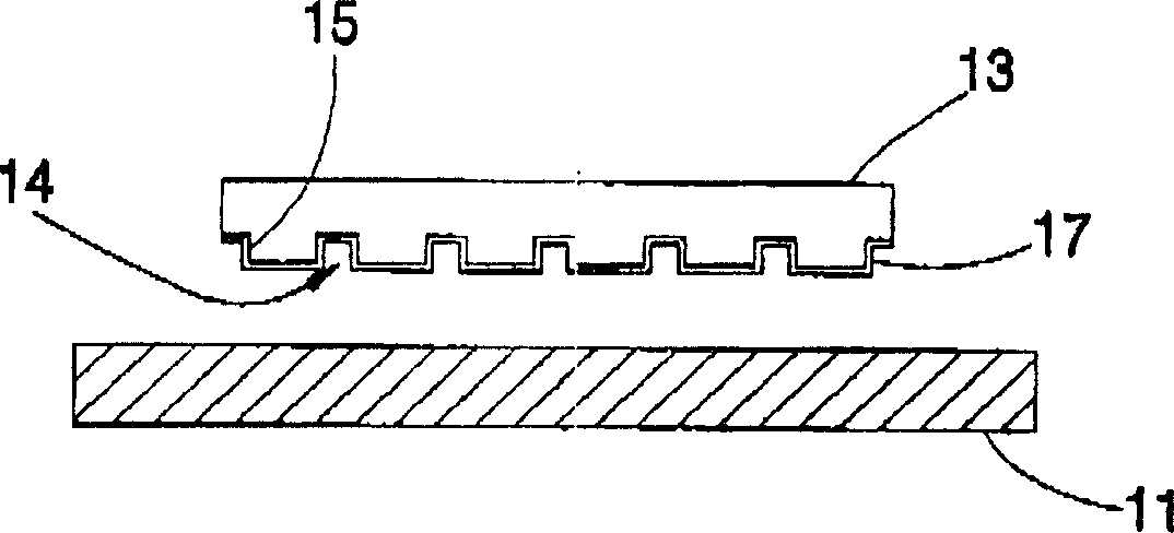
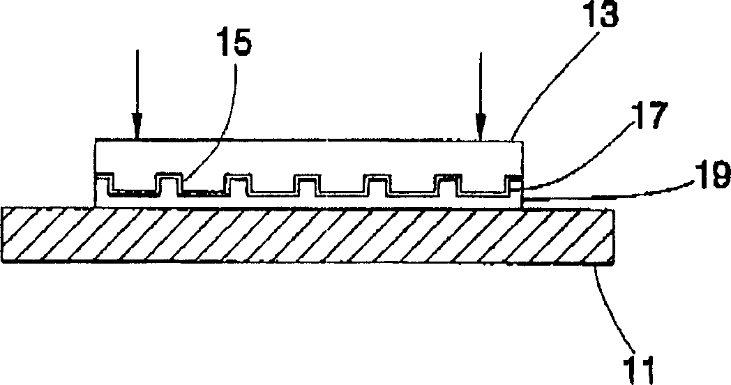
[0036] a) In a vacuum environment, a substrate 11 and a mold 13 are prepared. The mold 13 is in the shape of a transparent plate and is located above the substrate 11, and the bottom of the mold 13 has a pressing surface 14 on the surface of the pressing surface 14 Nano-embossing 15, with a layer of release agent 17 on the surface of the nano-embossing 15, in a state as figure 1 Shown

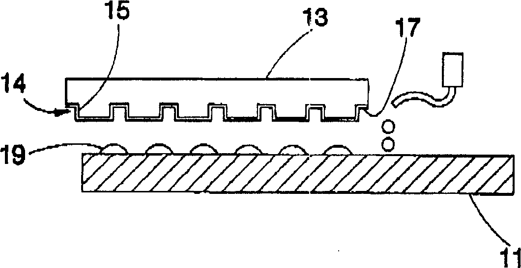
[0037] b) A liquid imprinting layer 19 is placed on the substrate 11. In this embodiment, it is a polymer. The imprinting layer 19 can be cured after being irradiated by ultraviolet light, and its state is as figure 2 As shown in the...


PUM


Abstract

The invention discloses a nanometer paster preparing method, which comprises the following steps: a) preparing one base plate and one die in the vacuum environment, wherein at least one of the base plate and die is clarity; the die is on base plate, which has one pressing surface; the pressing surface is installed nanometer emboss; the nanometer emboss installs release agent; b) the base plate is covered with liquid coining inlay which can be irradiated by ultraviolet light and then cure; c) the pressing surface of die presses base plate; the coining inlay is filled between nanometer emboss and base plate; d) ultraviolet irradiation makes ultraviolet transmit die or base plate to be clarity; irradiating the pressing inlay makes the pressing inlay cure; e) demoulding, the die is moved away the base plate; the pressing inlay forms line in respect of nanometer emboss; the pressing inlay is the nanometer paster.

Description

Technical field [0001] The present invention is related to nanotechnology, and in particular refers to a manufacturing method of nanometer stickers that can meet industrial mass production and low-cost requirements. Background technique [0002] According to the technology of manufacturing nano-stickers, LithographyTechniques is currently used to meet mass production and low-cost requirements. Among them, technologies with a line width resolution of less than 50 nanometers can meet future semiconductor integrated circuits, Electronic commercialization, optoelectronics industry, and manufacturing needs of magnetic nanodevices. [0003] Among the currently known technologies, there is a scanning electron beam plate printing technology (KCBeard, T. Qi. MRDawson, B. Wang. C. Li, Nature 368, 604 (1994).), with 10 nanometers However, because this technology is arranged in series in a point by point manner, its production speed is extremely low and cannot meet the needs of mass producti...

Claims


Application Information

Patent Timeline
Patent Type & Authority Applications(China)
IPC IPC(8): B29C59/02B29C41/12B29D15/00
CPCB82Y40/00B82Y10/00G03F7/0002
Inventor 赵治宇谢文俊
Owner CONTREL TECH CO LTD
Why Eureka
Try Eureka