Safety monitoring mechanism for wafer technique platform

A safety monitoring and process technology, applied in the fields of semiconductor/solid-state device manufacturing, instruments, electrical components, etc., can solve the problems of parts aging, wear, production and assembly, and increased wafer process defect rate.

Inactive Publication Date: 2006-10-11
泉胜科技股份有限公司
View PDF0 Cites 8 Cited by
  • Summary
  • Abstract
  • Description
  • Claims
  • Application Information

AI Technical Summary

Problems solved by technology

[0004] Regardless of the process platform mentioned above, a transfer device is used to carry the wafer and transfer the wafer between the reaction chambers, and the current transfer device is usually a robot arm, and the transfer device still exists The problem of parts aging, wear and assembly error, once the problem of part aging, wear and assembly error occurs in the transfer device, it will affect the production of the wafer, which may be sent into the reaction chamber or by the reaction. When the chamber is taken out, the wafer may be scratched due to contact with other components such as the entrance of the reaction chamber, the frame, etc., and the aging, wear, and manufacturing and assembly errors of the parts cannot suddenly occur in large numbers, but will gradually occur bit by bit. Therefore, it is very difficult to detect. It may be discovered in the inspection process after all the processes of the wafer are completed. During this period, the number of problematic wafers completed by the process platform may have been very large, so that it will make The defect rate in the wafer process has increased significantly

Method used


Image

  • Safety monitoring mechanism for wafer technique platform
  • Safety monitoring mechanism for wafer technique platform
  • Safety monitoring mechanism for wafer technique platform

Examples


Embodiment Construction

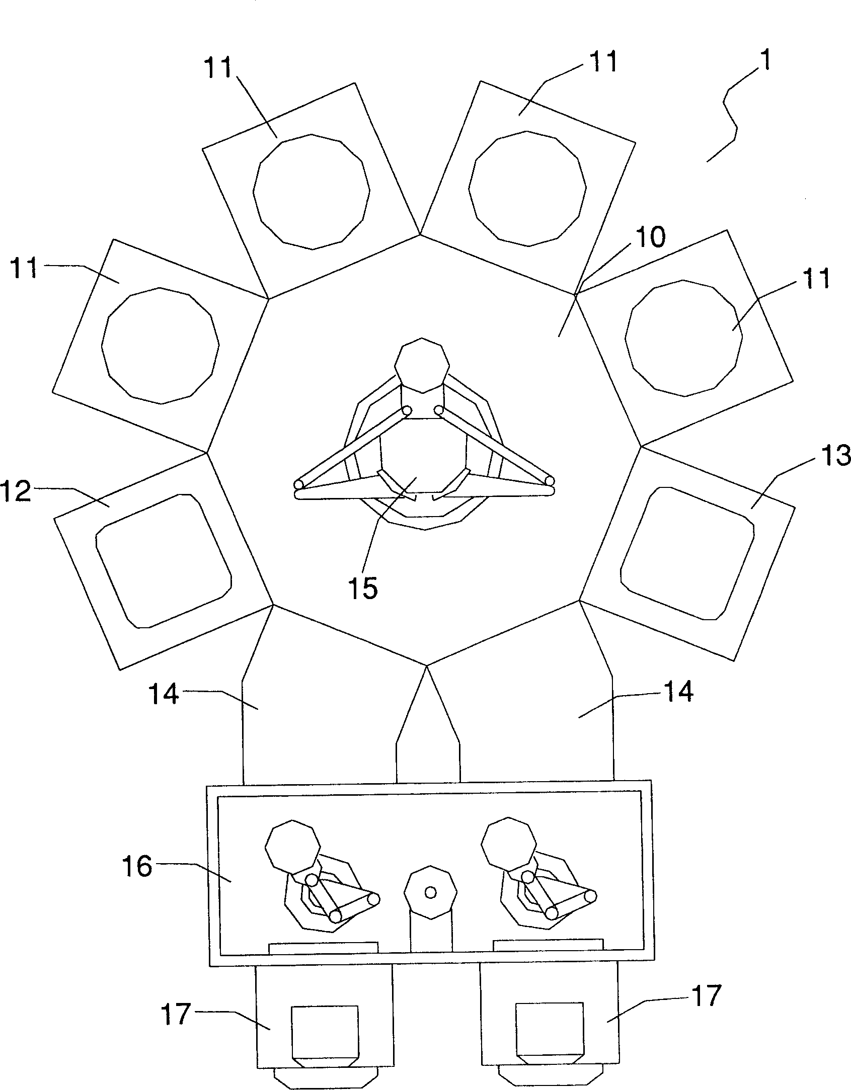
[0028] Please see figure 2 As shown, it is the first preferred embodiment of the safety monitoring mechanism of the wafer process platform of the present invention, including:

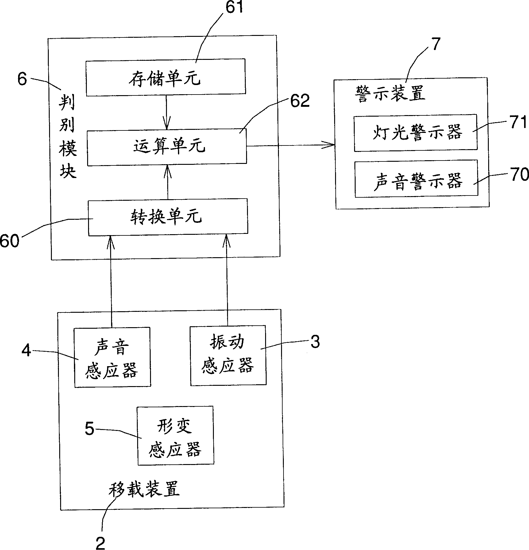
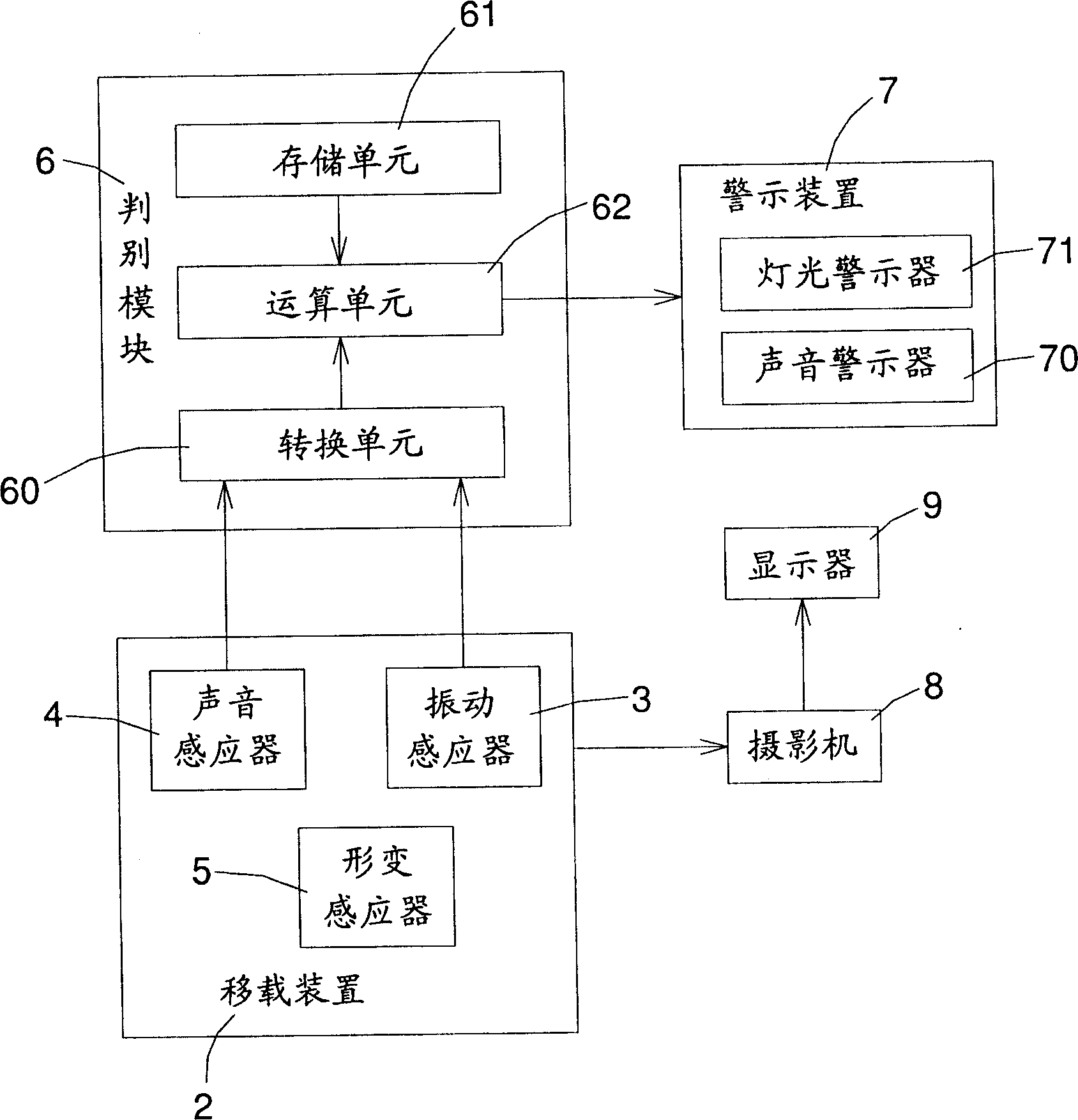
[0029] A vibration sensor 3 is arranged on the transfer device 2 of the wafer process platform for detecting the vibration generated when the transfer device 2 is in operation;

[0030] A sound sensor 4 is arranged on the transfer device 2 of the wafer process platform for detecting the sound generated when the transfer device 2 is in operation;

[0031] A deformation sensor 5 is arranged on the transfer device 2 of the wafer process platform for detecting the curvature or displacement generated when the transfer device 2 is in operation;

[0032] A discrimination module 6 includes a conversion unit 60, a storage unit 61 and a computing unit 62, the conversion unit 60 can be used to receive the vibration or vibration detected by the vibration sensor 3 or the sound sensor 4 or the deformation sensor 5...


PUM


Abstract

The related security monitor mechanism for a wafer technical platform comprises mainly: on the device for wafer transferring, a vibration or sound or deformation sensor to detect the corresponding quality, a decision module to receive and convert the former quality into digital signal for comparison and analysis with preset standard signal range, and an alert device to produce the sound and light when the detected signal over the standard or abnormal. Thereby, this invention can reduce undesirable-rate greatly and improves economic benefits.

Description

technical field [0001] The present invention relates to the technical field of a security monitoring mechanism for a semiconductor integrated circuit chip process platform, especially a chip that can be detected and eliminated in real time at the initial stage of process abnormalities, thereby greatly reducing the defect rate. The security monitoring mechanism of the process platform. Background technique [0002] The production of general semiconductor integrated circuit wafers (hereinafter referred to as wafers), from oxidation (Oxidation), diffusion (Diffusion), lithography (Photo), etching (Etch), chemical vapor deposition (CVD) to metal wire sputtering (Metal Sputter) Processes such as these need to be repeated many times. Therefore, in this diverse and complex wafer process, if a systematic and automated system is not used to integrate the front and rear related processes together, it will have a negative impact on product quality and production costs. It has a very l...

Claims


Application Information

Patent Timeline
Patent Type & Authority Applications(China)
IPC IPC(8): H01L21/00H01L21/66G06Q90/00
Inventor 黄裕鸿
Owner 泉胜科技股份有限公司
Why Eureka
Try Eureka