Technique and structure for making convex

A manufacturing process and technology of bumps, applied in semiconductor/solid-state device manufacturing, electrical components, electric solid-state devices, etc., can solve problems such as inability to provide connection between bumps 22 and wires 48, cracking, and low compression yield

Inactive Publication Date: 2006-11-15
ELAN MICROELECTRONICS CORPORATION
View PDF0 Cites 4 Cited by
  • Summary
  • Abstract
  • Description
  • Claims
  • Application Information

AI Technical Summary

Problems solved by technology

During lamination, the conductive particles 56 in the bump gap 54 are easily squeezed and deformed due to their large particle size, resulting in short circuit and leakage between adjacent bumps 22, resulting in low lamination yield.
If conductive particles 52 with a smaller particle size are used, a good connection between the bump 22 and the wire 48 cannot be provided, so the known technology has insurmountable difficulties
With the reduction of IC size and the demand for high I / O count, the bonding pads 14 of the IC are also reduced, and the effective area 32 is thus reduced, resulting in a reduction in the bonding yield and the conductive quality after bonding.
Furthermore, a natural disadvantage of the flip-chip package is that the mechanical strength of the edge region 58 of the bump 22 is weak, and it is easy to be broken due to lateral pulling.
However, in order to obtain a smaller roughness h on the surface of the bump 22, the height of the step 28 must be reduced, so the thickness of the sheath 16 is thinner, and the disadvantage of weaker mechanical strength cannot be overcome.

Method used


Image

  • Technique and structure for making convex
  • Technique and structure for making convex
  • Technique and structure for making convex

Examples


Embodiment Construction

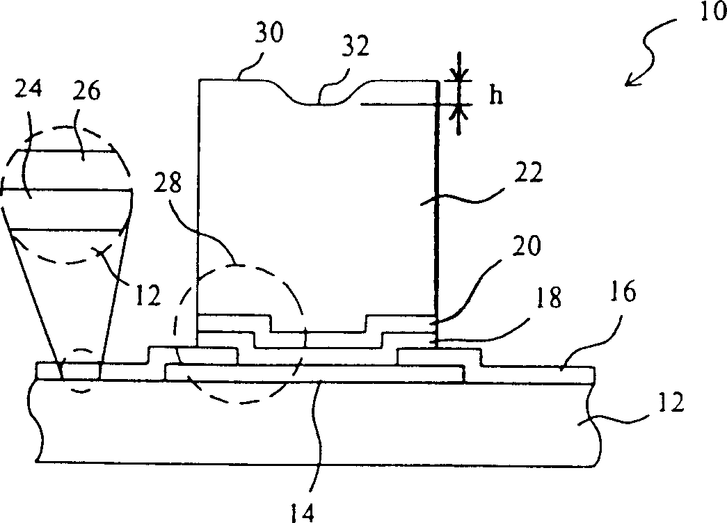
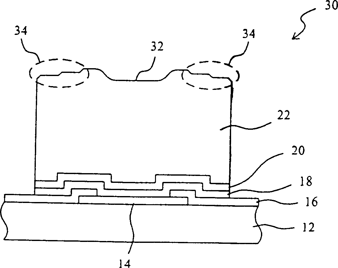
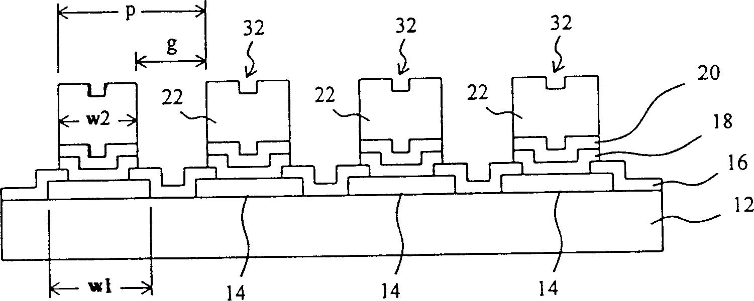
[0070] According to the present invention, a gold bump structure 60 such as Figure 6A and Figure 6B As shown, its top view is as Figure 7A and Figure 7B as shown, Figure 6A is a cross-sectional view in the X direction, Figure 6B is a cross-sectional view in the Y direction. refer to Figure 6A and Figure 6B , in the bump structure 60, the protective layer 64 with a planarized surface covers the bonding pad 62 of the substrate 12, the UBM18 and the gold film 20 are stacked on the bonding pad 62 and the protective layer 64, and the gold bump 66 is on the gold film 20 superior. The bonding pad 62 is made of aluminum, aluminum alloy, or other highly conductive metal or alloy. The protective layer 64 includes one or more layers of silicon dioxide, silicon nitride, or other highly chemically resistant materials or a combination thereof, to protect the circuitry in the underlying substrate 12 . UBM18 is mainly used to protect the bonding pad 62 to prevent various chem...


PUM


Abstract

This invention relates to cam creation technique and its structure. It includes a sheath with flat surface, the sheath is covered on a joint mat on the plaque to form a contact surface with one open through the sheath, and one cam on the contact surface and the flat surface is formed. The contact mat can be reduced because of the flat surface of the sheath. The mechanical strength of the sheath on the contact mat is strengthened; the cam will has large efficient area when stitching. Selecting space of different directivity conduction membrane is large, short circuit and electric leakage probability is little, so the stitching good ratio and conducting quality of the cam is improved.

Description

technical field [0001] The present invention relates to a manufacturing process and structure of a bump, in particular to a manufacturing process and structure of a planarized bump. Background technique [0002] Wire bonding, tape automatic bonding (TAB) and flip chip (flip chip) bonding are typical technologies for integrated circuit (IC) packaging. Generally speaking, wire bonding is used in low-density wiring packages with less than about 300 contacts, high-connection-density packages for TAB applications reach about 600 contacts, and flip-chip bonding provides higher connection density packages with more than 600 contacts. . Packages that use flip-chip bonding must first grow bumps on the bonding pads of the IC in order to attach chips to glass (Chip On Glass; COG), chip bonding circuit boards (Chip On Board; COB), and chip bonding. Lamination is performed in Chip On Film (COF) or other packaging procedures. In order to reduce telecommunication interference, increase ...

Claims


Application Information

Patent Timeline
Patent Type & Authority Applications(China)
IPC IPC(8): H01L21/28H01L21/44H01L21/60H01L21/768H01L23/48H01L23/522
CPCH01L24/11H01L2224/11H01L2224/16225H01L2224/32225H01L2224/73204H01L2924/14H01L2924/00H01L2924/00012
Inventor 胡钧屏陈正中蔡建文李育青
Owner ELAN MICROELECTRONICS CORPORATION
Why Eureka
Try Eureka