

GaN-based LED extension sheet and its preparation method
An LED epitaxial wafer and buffer layer technology, applied in electrical components, circuits, semiconductor devices, etc., can solve the problems of uneven current diffusion, affecting LED luminous efficiency and life, less hole injection, etc., to reduce interface resistance, The effect of increasing the external quantum efficiency of the LED and reducing the junction temperature of the LED
- Summary
- Abstract
- Description
- Claims
- Application Information
AI Technical Summary
Problems solved by technology
Method used
Image

Examples
Embodiment 1
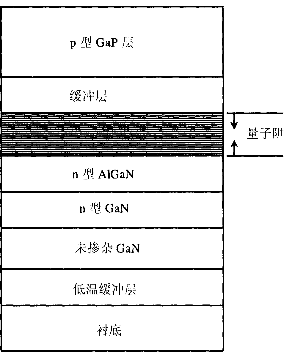
[0034] The structure of the new GaN-based LED epitaxial wafer is as follows: figure 1 As shown, from bottom to top are substrate, low temperature buffer layer, undoped GaN layer, n-type GaN:Si layer, n-type AlGaN:Si layer, quantum well, buffer layer, p-type GaP:Mg layer.
[0035] Its preparation method is:
[0036] 1) Use MOCVD dedicated to GaN, heat up to 1000°C and bake the substrate for 10 minutes in a hydrogen atmosphere;
[0037] 2) Lower the temperature to 480°C, and grow a GaN low-temperature buffer layer with a thickness of 30nm on the substrate;
[0038] 3) heating up to 1050° C., and growing an undoped GaN layer with a thickness of 2.0 μm;
[0039] 4) growing an n-type GaN:Si layer with a thickness of 2.0 μm at a temperature of 1050° C.;
[0040] 5) Growth of n-type Al with a thickness of 0.1 μm at a temperature of 1050°C 0.1 Ga 0.9 N: Si layer;
[0041] 6) Lower the temperature to 700°C to grow In x Ga yN / GaN multi-quantum well structure, the thickness of th...
Embodiment 2
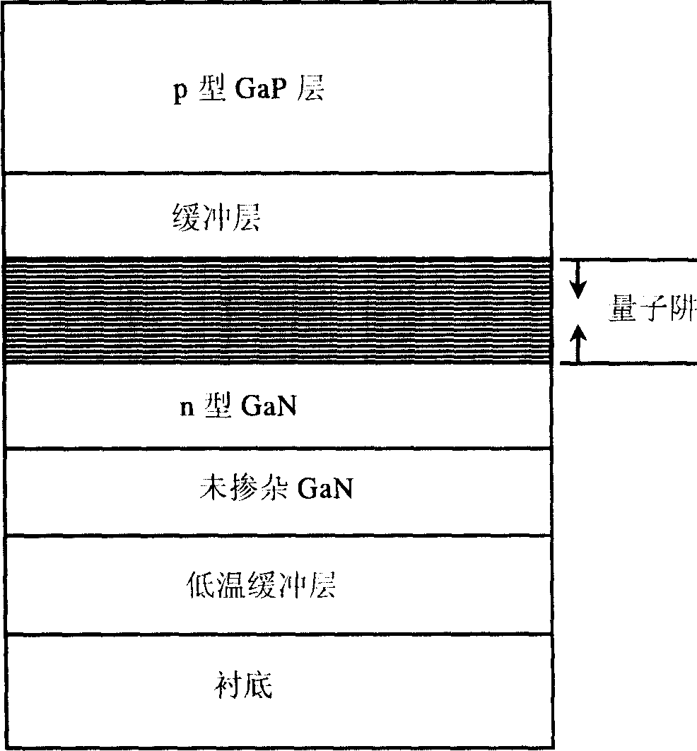
[0049] The structure of the new GaN-based LED epitaxial wafer is as follows: figure 2 As shown, from bottom to top are substrate, low temperature buffer layer, undoped GaN layer, n-type GaN:Si layer, quantum well, buffer layer, p-type GaP:Mg layer.
[0050] Its preparation method is:
[0051] 1) Use MOCVD dedicated to GaN, heat up to 1050°C and bake the substrate for 8 minutes in a hydrogen atmosphere;
[0052] 2) Lower the temperature to 510°C, and grow a GaN low-temperature buffer layer with a thickness of 25nm on the substrate;
[0053] 3) heating up to 1000° C., and growing an undoped GaN layer with a thickness of 2.5 μm;
[0054] 4) growing an n-type GaN:Si layer with a thickness of 1.0 μm at a temperature of 1000° C.;
[0055] 5) Lower the temperature to 600°C and grow an InGaN / GaN multi-quantum well structure. The thickness of the InGaN well layer is 4nm, and the thickness of the GaN barrier layer is 6nm; the In composition of the InGaN well layer is 0.25-0.5; the n...
Embodiment 3
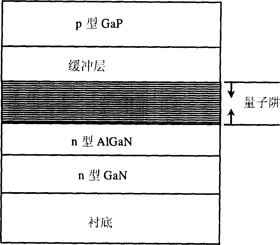
[0062] The structure of the new GaN-based LED epitaxial wafer is as follows: figure 1 As shown, from bottom to top are substrate, low temperature buffer layer, undoped GaN layer, n-type GaN:Si layer, n-type AlGaN:Si layer, quantum well, buffer layer, p-type GaP:Zn layer.
[0063] Its preparation method is:
[0064] 1) Use MOCVD dedicated to GaN, heat up to 1100°C and bake the substrate for 5 minutes in a hydrogen atmosphere;
[0065] 2) Lower the temperature to 550°C, and grow a GaN low-temperature buffer layer with a thickness of 20nm on the substrate;
[0066] 3) heating up to 1100°C, and growing an undoped GaN layer with a thickness of 1.5 μm;
[0067] 4) growing an n-type GaN:Si layer with a thickness of 3.0 μm at a temperature of 1100° C.;
[0068] 5) Growth of n-type Al with a thickness of 0.05 μm at a temperature of 1100°C 0.2 Ga 0.8 N: Si layer;
[0069] 6) Lower the temperature to 800°C and grow an InGaN / GaN multi-quantum well structure, the thickness of the InG...
PUM
 Abstract
Description
Claims
Application Information