Planar mono-silicon double-metal layer power device and its production

A dual-metal layer, power device technology, used in semiconductor/solid-state device manufacturing, electrical solid-state devices, semiconductor devices, etc., can solve problems such as high cost, large silicon wafer area, and unfavorable integrated circuit miniaturization, and achieve low cost, Good product quality and the effect of improving the performance of low capacitance and fast turn-on

Inactive Publication Date: 2007-01-17
NANKER GUANGZHOU SEMICON MFG
View PDF0 Cites 1 Cited by
  • Summary
  • Abstract
  • Description
  • Claims
  • Application Information

AI Technical Summary

Problems solved by technology

This kind of planar power device needs to form pads for gate, source and drain bonding wires on the outside of the main body of the power device, and heat dissipation needs to be considered, which requires a large area of ​​silicon wafers, which is not conducive to the miniaturization of integrated circuits, and the cost is also low. higher

Method used


Image

  • Planar mono-silicon double-metal layer power device and its production
  • Planar mono-silicon double-metal layer power device and its production
  • Planar mono-silicon double-metal layer power device and its production

Examples


Embodiment 1

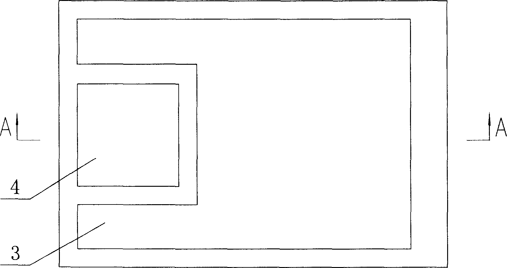
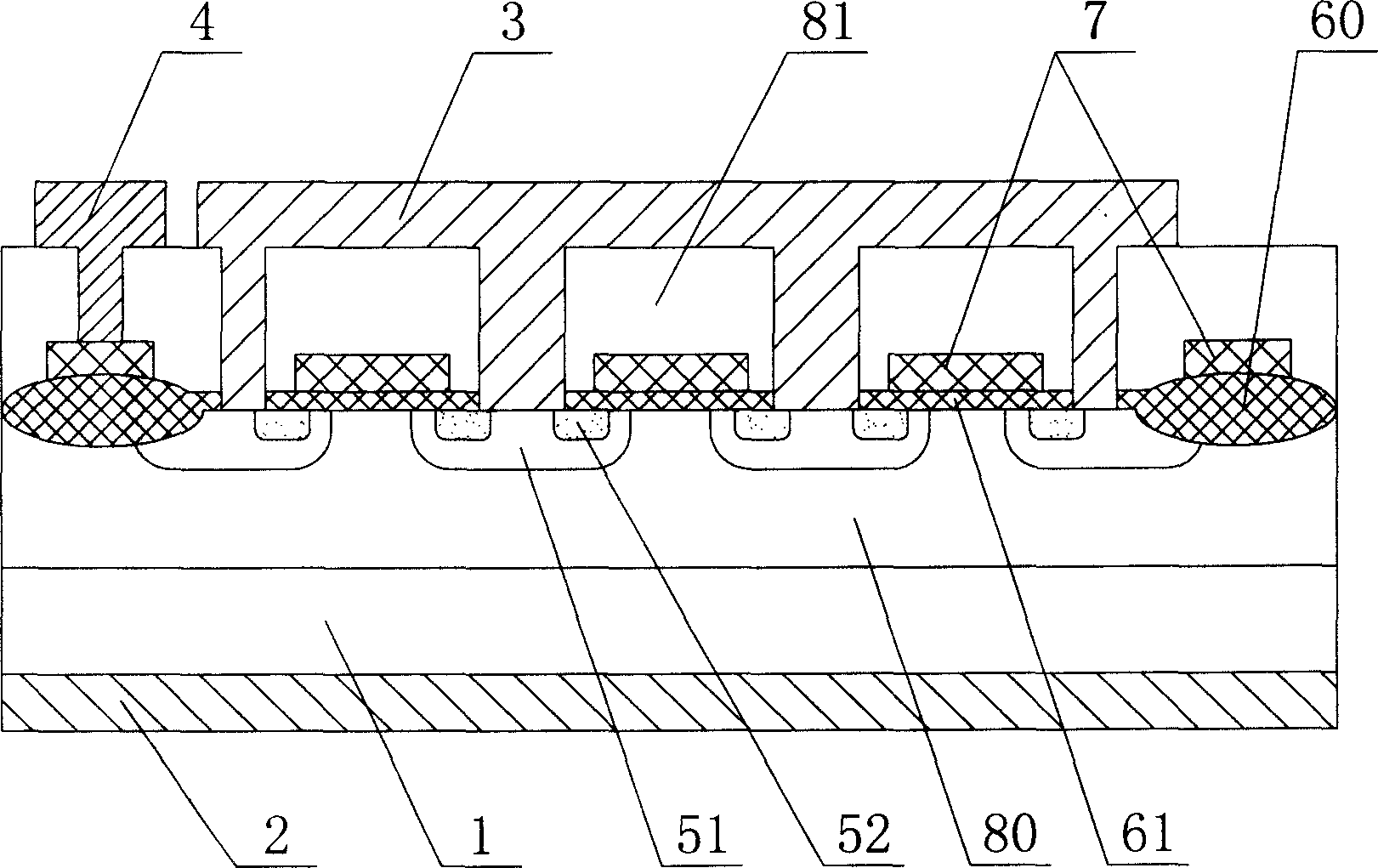
[0047] Such as Figure 5 to Figure 9 As shown, the planar single-silicon double-metal layer power device of this embodiment is an N-channel MOSFET, which includes an N-type silicon substrate 1, a P-type well region 90 formed in the silicon substrate 1, and a P-type well region 90 formed in the silicon substrate 1. The oxide layer I81 on the front side of the silicon substrate 1, the drain metal I2, source metal I3, and gate metal I4 located on the front side of the oxide layer I81, are implanted into the P+well contact region 50 in the silicon substrate 1 , N+ source region 52, N+ drain region 53, connecting the channel region 65 between the source region 52 and the drain region 53, growing on the gate oxide layer I60 and gate oxide layer II61 on the front side of the silicon substrate 1, The polysilicon gate 7 located on the gate oxide layer I60 and the gate oxide layer II61, the polysilicon gate 7 is distributed in stripes, and there are five stripes and one annular through ...

Embodiment 2

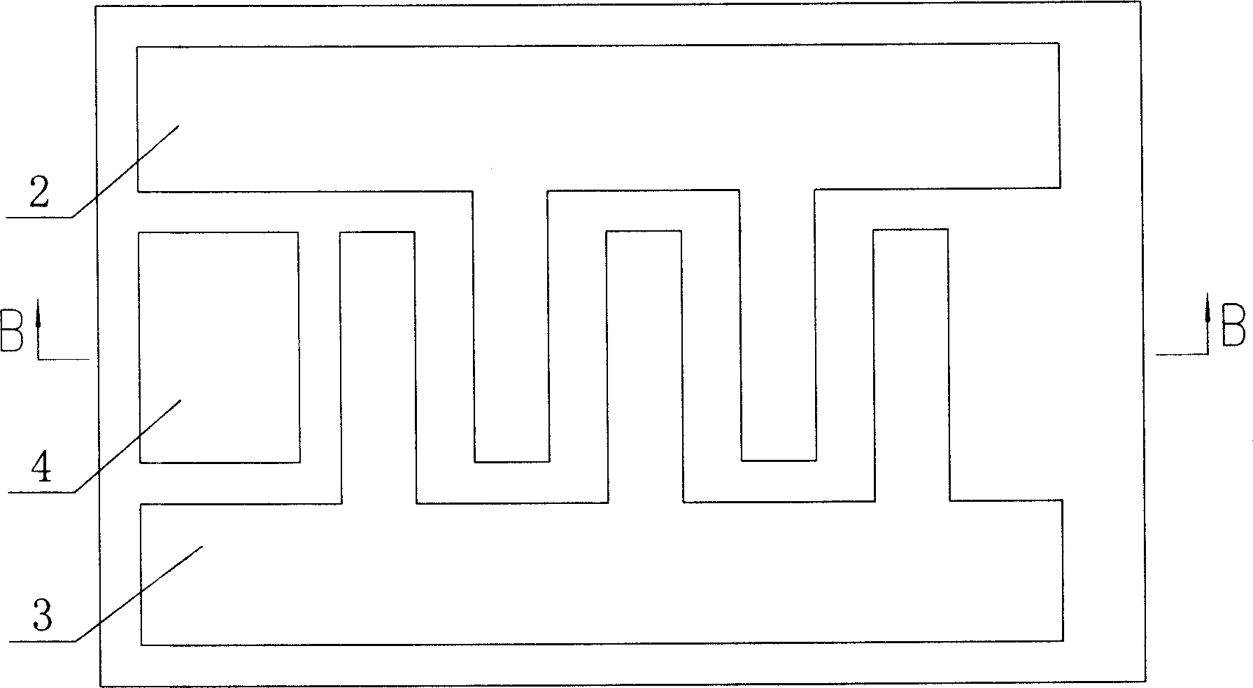
[0061] Such as Figure 10 ~ Figure 12 As shown, the planar single-silicon double-metal layer power device of this embodiment is a P-channel MOSFET. The through-holes I83 through which the metal I2 and the source metal I3 are in contact with the silicon substrate 1 are also distributed in grid-like intervals. The silicon substrate 1 is an N-type substrate, the well region 90 is an N-type well region, the well contact region 50 is an N+ well contact region, the source region 52 is a P+ source region, and the drain region 53 It is the P+ drain area. The drain metal I2, the source metal I3, the gate metal I4, the drain metal II2', the source metal II3', and the gate metal II4' are copper. Other features are the same as in Embodiment 1.

[0062] The difference between the manufacturing method of the planar single-silicon double-metal layer power device of this embodiment and the first embodiment is that:

[0063] Step (b) Forming the well region: Implanting phosphorus N-type do...

Embodiment 3

[0069] The planar single-silicon double-metal layer power device of this embodiment is an N-channel MOSFET, and it differs from Embodiment 1 in that the gate metal II4' is connected to the gate metal II4' through another through hole II84. Metal I4 is connected and connected to other circuits without forming a pad. The silicon substrate 1 is a P-type substrate, the well region 90 is a P-type well region, the well contact region 50 is a P+ well contact region, the source region 52 is an N+ source region, and the drain region 53 It is the N+ drain region. The drain metal I2, the source metal I3, the gate metal I4, the drain metal II2', the source metal II3', and the gate metal II4' are silicon aluminum alloys. Other features are the same as in Embodiment 1.

[0070] The difference between the manufacturing method of the planar single-silicon double-metal layer power device of this embodiment and the first embodiment is that:

[0071] Step (b) forming a well region: inject bor...


PUM


Abstract

A plane single silicon bimetal layer power parts and the manufacture method, the power parts includes: the silicon underlay; the two oxidation layers that forms at the trap area in the silicon underlay and the front surface of the silicon underlay; the leaking pole metal, the source pole metal and the grid metal that are located at the front surface of the two oxidation layers; the trap touching area, the source area, the leaking area and the channel area that is established in the silicon underlay; forms a grid oxidation layer at the front surface of the silicon underlay; the multi-crystal grid located on the oxidation layer; the two oxidation layers with several holes respectively; the filling holes of the leaking pole metal, the source pole metal and the grid metal on the front surface of the two oxidation layers connect with the leaking area, the trap touching area, the source area and the multi-crystal silicon grid. The manufacture method includes the grid oxidation layer, the trap area, the channel area, the multi-crystal silicon grid, the trap touching area, the source area, the leaking area, the oxidation layer and the metal layer. The invention is low cost, small engrossing area, small grid capacitance, and easy integration.

Description

technical field [0001] The invention relates to a planar single-silicon double-metal layer power device and a manufacturing method. Background technique [0002] "MOSFET" is the abbreviation of "metal-oxide-semiconductor field effect transistor" in English, which means "metal oxide semiconductor field effect transistor", and its principle is the basis of all modern integrated circuit chips. A MOSFET device consists of three basic parts: source (S), gate (G) and drain (D). If a voltage is applied to the gate, when the voltage is greater than the MOSFET’s turn-on voltage V TH , a current path is formed between the source and the drain; if there is no voltage on the gate or the applied voltage is less than the MOSFET’s turn-on voltage V TH , then the transistor will block this path, that is, it will be in a closed state. Using this function, multiple transistors can be combined to form various circuits. Small-signal MOSFETs are mainly used for signal...

Claims


Application Information

Patent Timeline
Patent Type & Authority Applications(China)
IPC IPC(8): H01L29/78H01L29/40H01L27/04H01L21/336H01L21/28H01L21/822
Inventor 吴纬国
Owner NANKER GUANGZHOU SEMICON MFG
Why Eureka
Try Eureka