TAB tape carrier

A carrier and strip-shaped technology, which is applied in the direction of electric solid devices, semiconductor devices, semiconductor/solid-state device components, etc., can solve the problem of difficult to ensure the gap between semiconductor elements and TAB tape carriers, the gap of sealing resin, and the difficulty of filling and sealing Resin and other problems, to achieve a firm connection, improve adhesion, and inhibit the effect of sinking

Inactive Publication Date: 2007-01-31
NITTO DENKO CORP
View PDF1 Cites 7 Cited by
  • Summary
  • Abstract
  • Description
  • Claims
  • Application Information

AI Technical Summary

Problems solved by technology

[0008] However, if the above-mentioned crimping is performed, when the conductor pattern is miniaturized, since the contact area between the conductor pattern and the insulating base layer decreases, the surface pressure on the insulating base layer of the conductor pattern increases. When the surface layer of the insulating base layer is formed of a thermoplastic polyimide resin layer to improve the adhesion with the conductor pattern, it is difficult to secure the tape shape between the semiconductor element and the TAB because the conductor pattern sinks into the surface layer. gap between carriers
In this case, it is difficult to fill the sealing resin, or even if the sealing resin can be filled, there may be a problem that voids appear in the sealing resin

Method used


Image

  • TAB tape carrier
  • TAB tape carrier
  • TAB tape carrier

Examples


Embodiment 1

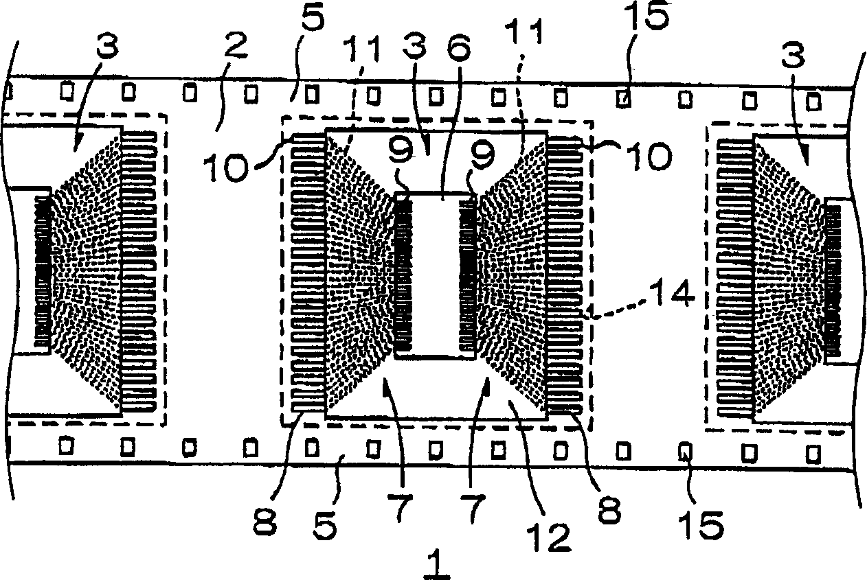
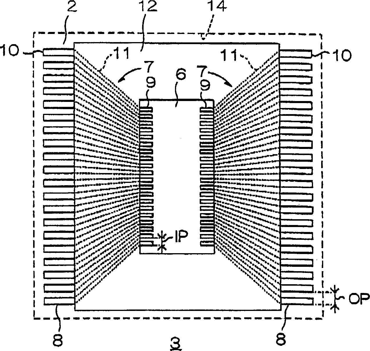
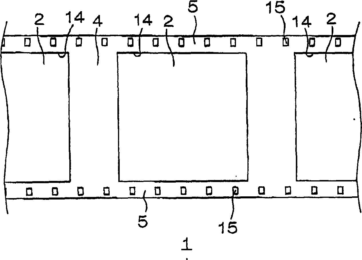
[0091] In this Example 1, four rows of tape carriers for TAB with a width of 48 mm were simultaneously produced on a reinforcement layer with a width of 250 mm.

[0092] First, as a reinforcing layer, prepare stainless steel (SUS304) with a thickness of 20 μm (reference Figure 4 (a)), on this reinforcing layer, coat polyamic acid resin solution, make it heat curing after drying, form the thermosetting polyimide resin layer that thickness is 20 μm (refer to Figure 4 (b)). In addition, the coefficient of linear expansion of this thermosetting polyimide resin layer was 20 ppm / °C.

[0093] Next, on the thermosetting polyimide resin layer, apply a thermoplastic polyimide resin solution mainly composed of aliphatic polyimide, and dry it to form a thermoplastic polyimide resin with a thickness of 1 μm. layer (reference Figure 4 (c)). In addition, the glass transition temperature of this thermoplastic polyimide resin layer was 300 degreeC.

[0094] In this way, an insulating b...

Embodiment 2、3 and comparative example 1

[0103] A tape-shaped carrier for TAB was obtained in the same manner as in Example 1, except that the thickness of the thermoplastic polyimide resin layer was 3 μm in Example 2, 4 μm in Example 3, and 5 μm in Comparative Example 1.

[0104] evaluate

[0105] In the mounting portion of the tape carrier for TAB obtained in Examples 1 to 3 and Comparative Example 1, a semiconductor element provided with gold bumps was mounted. In the mounting of the semiconductor element, gold bumps are opposed to inner leads covered with tin plating, and crimping is performed at a mounting temperature (temperature of crimping equipment) of 325°C and a mounting load of 130N. After crimping, the amount of dishing of the insulating base layer was measured. The results are shown in Table 1.

[0106] After that, the gap between the semiconductor element and the mounting portion of the tape carrier for TAB is filled with a liquid primer and the sealing resin (liquid Anta-fil sealing resin) is filled...


PUM


Abstract

To provide a TAB tape carrier that can provide improved adhesion of a conductive pattern to an insulating base layer, while strengthening a connection between gold terminals of a semiconductor device and connection terminals covered with a tin plating layer, and can prevent the conductive pattern from sinking into the insulating base layer. In the TAB tape carrier 1, an insulating base layer 2 is formed by laminating a thermoplastic polyimide resin layer 2b of 4µm thick or less on a thermosetting polyimide resin layer 2a, and a conductive pattern 7 having inner leads 9 covered with a tin plating layer 13 is formed on a surface of the thermoplastic polyimide resin layer 2b. In this TAB tape carrier 1, even when the gold terminals 22 of the semiconductor device 21 are press-bonded to the inner leads 9 covered with the tin plating layer 13 at high temperatures and pressures, the conductive pattern 7 can be prevented from sinking into the insulating base layer 2.

Description

technical field [0001] The present invention relates to a tape carrier for TAB, and more particularly to a tape carrier for TAB for mounting a semiconductor element by a TAB method. Background technique [0002] Tape carrier for TAB is a tape carrier on which semiconductor elements are mounted by the TAB (Tape Automated Bonding) method, and is widely used in the field of electronic components. [0003] As such a tape-shaped carrier for TAB, there is known a tape-shaped carrier in which a conductor pattern formed of copper foil is formed on an insulating base layer formed of polyimide resin (for example, refer to Japanese Patent Laid-Open No. 2004 - Bulletin No. 134442). [0004] In this TAB tape carrier, the conductor pattern is formed as a plurality of wiring patterns integrally formed with inner leads, outer leads, and relay leads, and the inner leads and outer leads are covered with nickel plating and gold plating. [0005] The semiconductor element is mounted on the ta...

Claims


Application Information

Patent Timeline
Patent Type & Authority Applications(China)
IPC IPC(8): H01L23/498H01L23/495H05K1/02
CPCH01L23/49894H01L2224/73204H01L2224/16225H01L23/4985H01L23/48
Inventor 中村圭石丸康人
Owner NITTO DENKO CORP
Why Eureka
Try Eureka