Organic light-emitting diodes and an arrangement with several organic light-emitting diodes

A light-emitting diode, organic technology, applied in the direction of organic semiconductor devices, electric solid-state devices, semiconductor devices, etc., can solve the problems of high reflectivity, hindering the selection of substrates, etc.

Inactive Publication Date: 2007-02-07
NOVALED GMBH
View PDF3 Cites 2 Cited by
  • Summary
  • Abstract
  • Description
  • Claims
  • Application Information

AI Technical Summary

Problems solved by technology

A further disadvantage of conventional organic light-emitting diodes is the often chosen arrangement with a transparent substrate: in this case the light emission of the light-emitting diode is achieved through transparent electrodes and the substrate, while the oppositely arranged contacts (in most cases the substrate) are Opaque and highly reflective in the relevant spectral region
Subsequently, for this application, highly transparent substrates and transparent contact layers are necessary, which in many cases limit the choice of substrates to a large extent and prevent the choice of particularly inexpensive substrates

Method used


Image

  • Organic light-emitting diodes and an arrangement with several organic light-emitting diodes
  • Organic light-emitting diodes and an arrangement with several organic light-emitting diodes
  • Organic light-emitting diodes and an arrangement with several organic light-emitting diodes

Examples


Embodiment 1

[0063] An embodiment of a blue emitting OLED includes the following layers:

[0064] 1 substrate, aluminum foil

[0065] 2 silver layers, sputtered

[0066] 3 Hole transport layer: Spiro-TTB, p-doped with 2% NDP-2, 25nm thick

[0067] 4 electron blocking layer, Spiro-TAD, 10nm

[0068] 5 emitter layer: blue emitter, 20nm

[0069] 6 electron transport layer, BPhen, 10nm

[0070] 7 Electron transport layer, BPhen, n-doped with Cs at a ratio of 1:1, 130nm

[0071] 8 transparent cathodes, Ag vapor deposited, 15nm

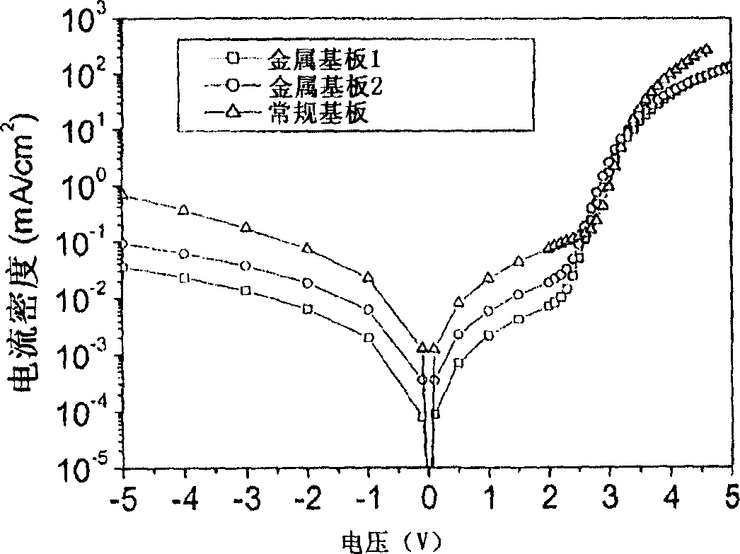
[0072] figure 1 The current-voltage characteristic curves (squares and circles) of two organic light-emitting elements of this type are shown; in comparison, a similar element realized on a high-quality glass substrate with clean room conditions is shown. The resulting Cr / Ag contacts. It is clear that these OLEDs have significantly better barrier characteristic curves. The surprising aspect here is that the effect requires only an unusually thick electron-trans...

Embodiment 2

[0074] An embodiment of a green emitting OLED comprises the following layers:

[0075] 10 substrates, aluminum foil

[0076] 11 silver layers, sputtered

[0077] 12 Hole transport layer: Spiro-TTB, p-doped with 2% NDP-2, 48nm thick

[0078] 13 electron blocking layer, Spiro-TAD, 10nm

[0079] 14 Emitter layer I, TCTA: Ir(ppy) 3 (9%), 5nm

[0080] 15 Emitter layer II, TPBI: Ir(ppy) 3 (9%), 10nm

[0081] 16 electron transport layer, BPhen, 10nm

[0082] 17 Electron transport layer, BPhen, n-doped with Cs at a ratio of 1:1, 130nm

[0083] 18 transparent cathodes, Ag vapor deposited, 15nm

[0084] 19 Overlay: Spiro-TTB, 90nm

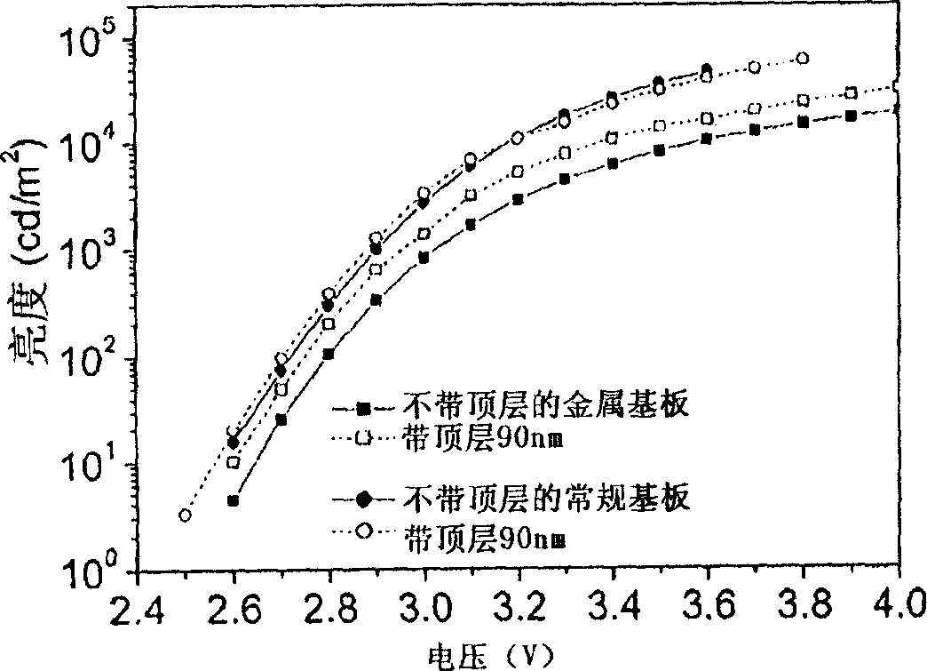
[0085] figure 2 The luminance-voltage characteristic curves of two organic light-emitting elements according to the second embodiment of the invention are shown (squares and circles, each with and without layer 19 ). 100Cd / m has been obtained at 2.9V 2 Brightness at 10,000Cd / m 2 The maximum performance efficiency is 501m / W. This demonstrates t...

Embodiment 3

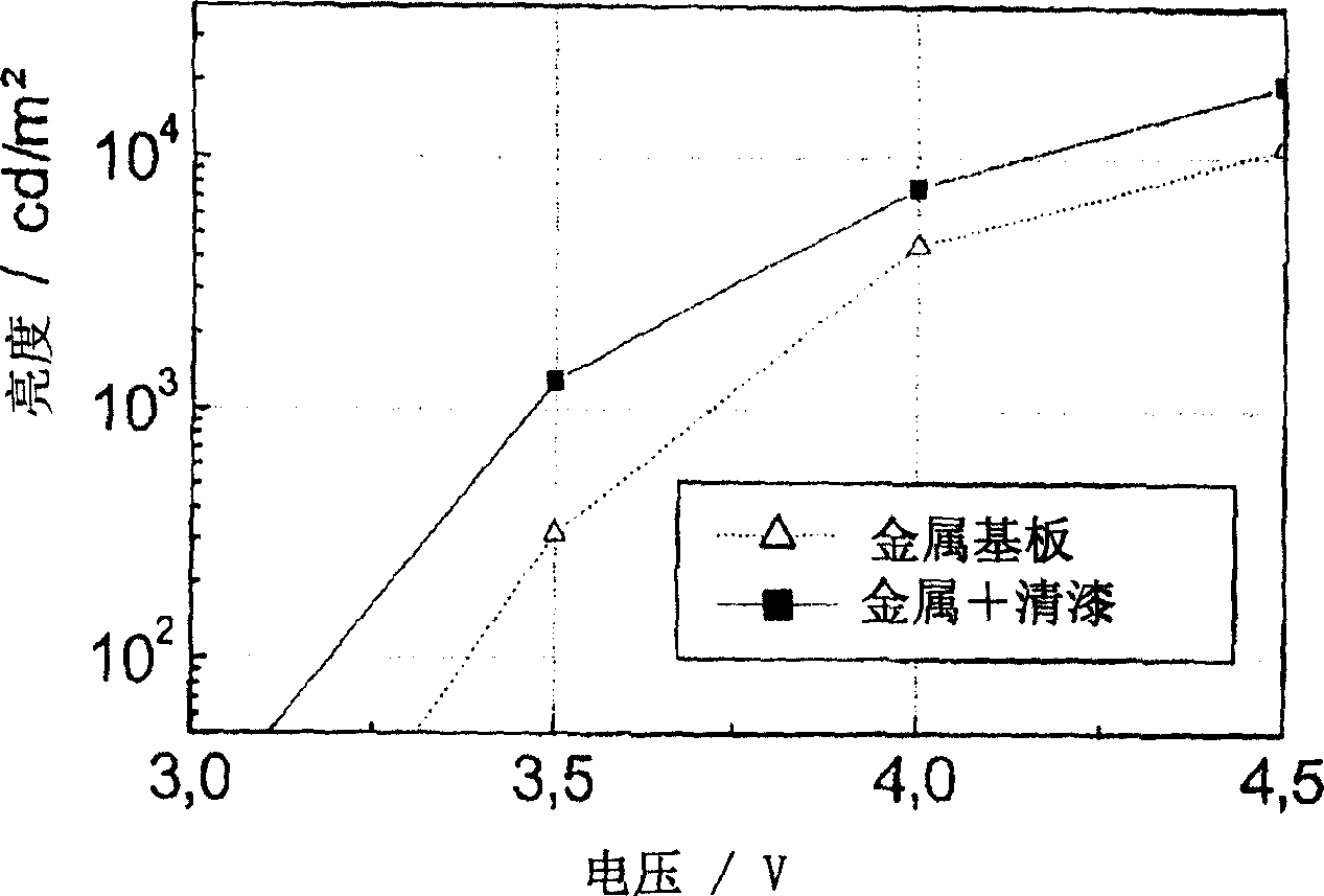
[0088] In Example 3, it is shown how an additional layer of varnish on a metal substrate contributes to lower leakage current and subsequently improved electrical performance. At the same time, a thick p-side is used, which helps to make the surface more uniform. For this purpose, image 3 Two OLEDs having structures similar in design, one formed with smoothing layer 21 and the other formed without smoothing layer 21 were compared.

[0089] 20 substrates, aluminum foil

[0090] 21 layers of smoothing, varnish (optional)

[0091] 22 silver layers, sputtered

[0092]23 Hole transport layer: MeO-TPD, p-doped with 4% F4-TCNQ, 150nm thick

[0093] 24 electron blocking layer, Spiro-TAD, 10nm

[0094] 25 luminescent layers, TCTA: Ir(ppy) 3 (8%), 20nm

[0095] 26 electron transport layer, BPhen, 10nm

[0096] 27 Electron transport layer, BPhen, n-doped with Cs at a ratio of 1:1, 30nm

[0097] 28 transparent cathodes, Ag vapor deposited, 15nm

[0098] From image 3 As can be...


PUM


Abstract

Organic light-emitting diode with a layer arrangement which comprises an electrode, a counter electrode and an organic layer sequence arranged between the electrode and the counter electrode, where the organic layer sequence is arranged on a metal substrate and one or several organic transport layers containing in each case an admixture for increasing the electric conductivity and which are formed with at least one of the features from the following group of features: charge carrier transporting and charge carrier injecting.

Description

technical field [0001] The invention belongs to the field of electroluminescent light-emitting devices. Background technique [0002] Since the demonstration of low operating voltage by Tang et al. (C.W.Tang et al.: Appl. Phys. Lett.51(12), 913(1987)), organic light-emitting diodes (OLEDs) have become the preferred choice for realizing large-area displays and lighting elements. Promising candidates. They consist of a series of thin layers (typically 1 nm to 1 μm) of organic materials which are preferably spin-coated or vapor-deposited in vacuum in their polymeric form. After being electrically contacted by conductive layers, they form various components such as light-emitting diodes, displays and lighting elements. With their respective properties, they bring competition to components built on organic layers. [0003] In the case of organic light-emitting diodes, an externally applied voltage results in the injection of charge carriers (electrons from one side and holes f...

Claims


Application Information

Patent Timeline
Patent Type & Authority Applications(China)
IPC IPC(8): H01L51/50H01L27/32
CPCH01L51/52H01L27/3281H01L51/0052H01L51/0059H01L51/0062H01L51/0085H01L51/5052H01L51/5203H01L2251/5315H01L2251/5338H10K59/17H10K85/649H10K85/615H10K85/631H10K85/342H10K50/155H10K50/165H10K50/80H10K50/805H10K2102/3026H10K2102/311H10K71/16
Inventor 卡尔斯滕·沃尔泽泰贾·罗赫黄强卡尔·利奥
Owner NOVALED GMBH
Why Eureka
Try Eureka