Surface plasmon resonance sensor

A resonant sensor, surface plasmon technology, applied in instruments, scientific instruments, measuring devices, etc., can solve the problem of not removing the solution part, etc.

Inactive Publication Date: 2007-02-21
ORMON CORP
View PDF0 Cites 21 Cited by
  • Summary
  • Abstract
  • Description
  • Claims
  • Application Information

AI Technical Summary

Problems solved by technology

[0008] But when figure 1 In the shown surface plasmon resonance sensor 1, since it is affected by a change in the refractive index at about 200 nm away from the metal thin film, there is a problem that not only the change in the refractive index due to the interaction of living molecules immobilized on the metal thin film, but also the Changes in the refractive index due to changes in the concentration, pH, temperature, etc. of the solution are also detected as noise
[000...

Method used


Image

  • Surface plasmon resonance sensor
  • Surface plasmon resonance sensor
  • Surface plasmon resonance sensor

Examples


Embodiment 1

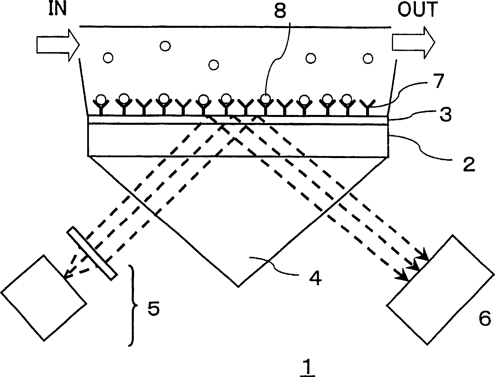
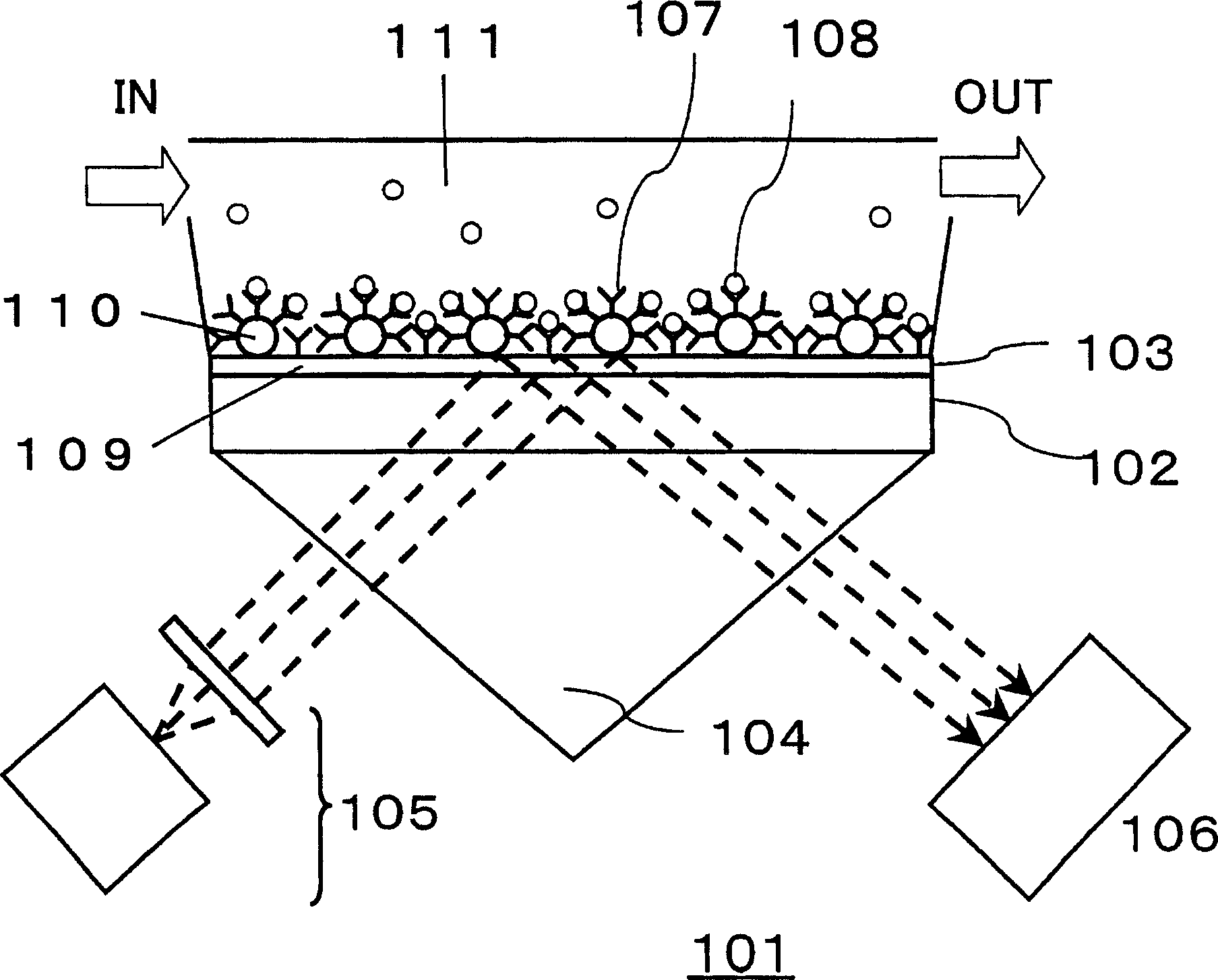
[0036] image 3 It is a schematic side view of the surface plasmon resonance sensor 101 according to the first embodiment of the present invention. The surface plasmon resonance sensor 101 has: a substrate 102 made of glass or the like; a metal layer 103 formed on the substrate 102; a prism 104 arranged on the side of the substrate 102 where the metal layer 103 is not formed; an optical system 105 for incident light at the interface; and a photodetector 106 for measuring the intensity of light reflected at the interface between the metal layer 103 and the substrate 102 . The optical system 105 may be configured to enter light of a certain wavelength at various incident angles, or may be configured to incident light of various wavelengths at certain incident angles.

[0037] In the present embodiment, the metal layer 103 is composed of a flat portion 109 formed in a film shape and metal particles 110 arranged at intervals, and the flat portion 109 is exposed between adjacent m...

Embodiment 2

[0053] Figure 9 It is a schematic side view of the surface plasmon resonance sensor 201 according to the second embodiment of the present invention. The structure of the metal layer 103 of this embodiment is different from that of the first embodiment. The metal layer 103 of this embodiment forms a metal thin film on the flat surface of the substrate 102 , and fine unevenness is formed on the metal thin film by etching or the like. Wherein, the concave portion is formed not to penetrate the metal thin film. When such a metal layer 103 is used, the electric field is localized in the vicinity of the concave portion or the convex portion, so that the same effect as that of the first embodiment can be obtained.

[0054] In addition, the shape and arrangement interval of the minute unevenness are not limited to Figure 9 The manner shown can be selected appropriately.

Embodiment 3

[0056] Figure 10 It is a schematic side view of the surface plasmon resonance sensor 301 according to the third embodiment of the present invention. The structures of the substrate 102 and the metal layer 103 of this embodiment are different from those of the first embodiment. In this embodiment, a plurality of micro-protrusions or micro-recesses are formed at intervals on the surface of the substrate 102, and the metal layer 103 is formed on the substrate 102 to reflect the shape of the micro-protrusions or micro-recesses. Even when such a metal layer 103 is used, the electric field is still localized in the vicinity of the concave portion or the convex portion, so the same effect as that of the first embodiment can be obtained.

[0057] The substrate 102 with fine unevenness formed on the surface used in this embodiment can be created and reproduced by taking a model of a living body molecule such as metal fine particles or protein.


PUM


Abstract

A surface plasmon resonance sensor comprising a chip having a substrate (102) and a metal layer (103), a prism (104), an optical system (105) becoming a light source, and a photodetector (106), wherein the metal layer (103) consists of a flat part (109) in the form of a thin film, and protrusions consisting of fine metal particles (110) or the like arranged at intervals. When light impinges on such a metal layer (103), a resonance angle caused by the flat part (109) and each protrusion is attained. Variation in the refractive index of a medium touching the metal layer can be detected from the resonance angle.

Description

technical field [0001] The present invention relates to a surface plasmon resonance (SPR: surface plasmon resonance) sensor, more specifically to a surface plasmon resonance sensor suitable for detecting the interaction of living molecules such as protein and DNA. Background technique [0002] In recent years, surface plasmon resonance sensors have been used as sensors for detecting the presence or degree of biomolecular interactions. [0003] figure 1 A conventional surface plasmon resonance sensor 1 is shown. The surface plasmon resonance sensor 1 has: a substrate 2 made of glass or the like; a metal thin film 3 formed on the substrate 2; a prism 4 arranged on the side of the substrate 2 where the metal thin film 3 is not formed; 3 and the interface of the substrate 2, an optical system 5 for incident light; a photodetector 6 for measuring the intensity of light reflected at the interface of the metal thin film 3 and the substrate 2. The metal thin film 3 is in contact ...

Claims


Application Information

Patent Timeline
IPC IPC(8): G01N21/55G01N21/27
CPCG01N21/554Y10T428/31678
Inventor 西川武男松下智彦青山茂乗冈茂巳和沢铁一
Owner ORMON CORP
Why Eureka
Try Eureka