
Eureka
For R&D, Eureka makes reading and utilizing patents & technical documents easy.
Eureka AIR
Designed for self-driven R&D workflows. Generate viable solutions, solve complex R&D challenges, empower your innovation with AI.

Eureka Materials
Designed for material experts only. Revolutionize your material R&D, from search, analyze, to developing new materials.

TechResearch
Generate reliable direction feasibility study reports for your R&D in just a few steps.

TechSeek
Discover and master advanced knowledge NOW. Basics, ideas, possibilities, all at once.

TechMind
As an expert in R&D Theories, TechMind can generates customized viable solutions instantly.

TechRisk
Analyze your overall solution with one click, know your potential R&D risks in advance.

TechMonitor
Get weekly tech updates, stay abreast of the latest tech innovations and key insights.
Package structure and method for thermo-optical switch array/modulator
A thermo-optic modulator and thermo-optic switch technology, which is applied in the field of device packaging, can solve the problems of expensive needs, expensive integrated circuit chips, and poor heat dissipation.
- Summary
- Abstract
- Description
- Claims
- Application Information
AI Technical Summary
Problems solved by technology
Method used
Image

Examples
Embodiment Construction
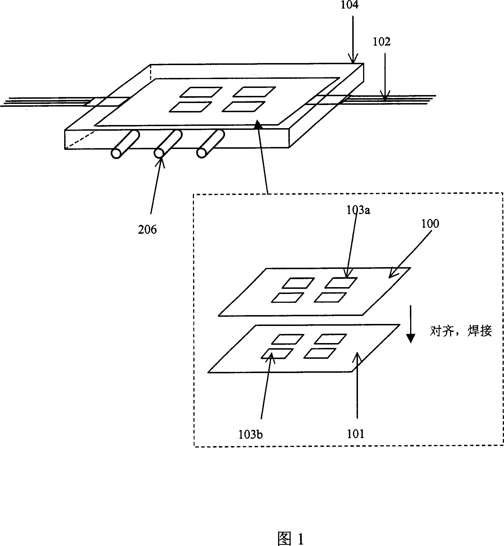
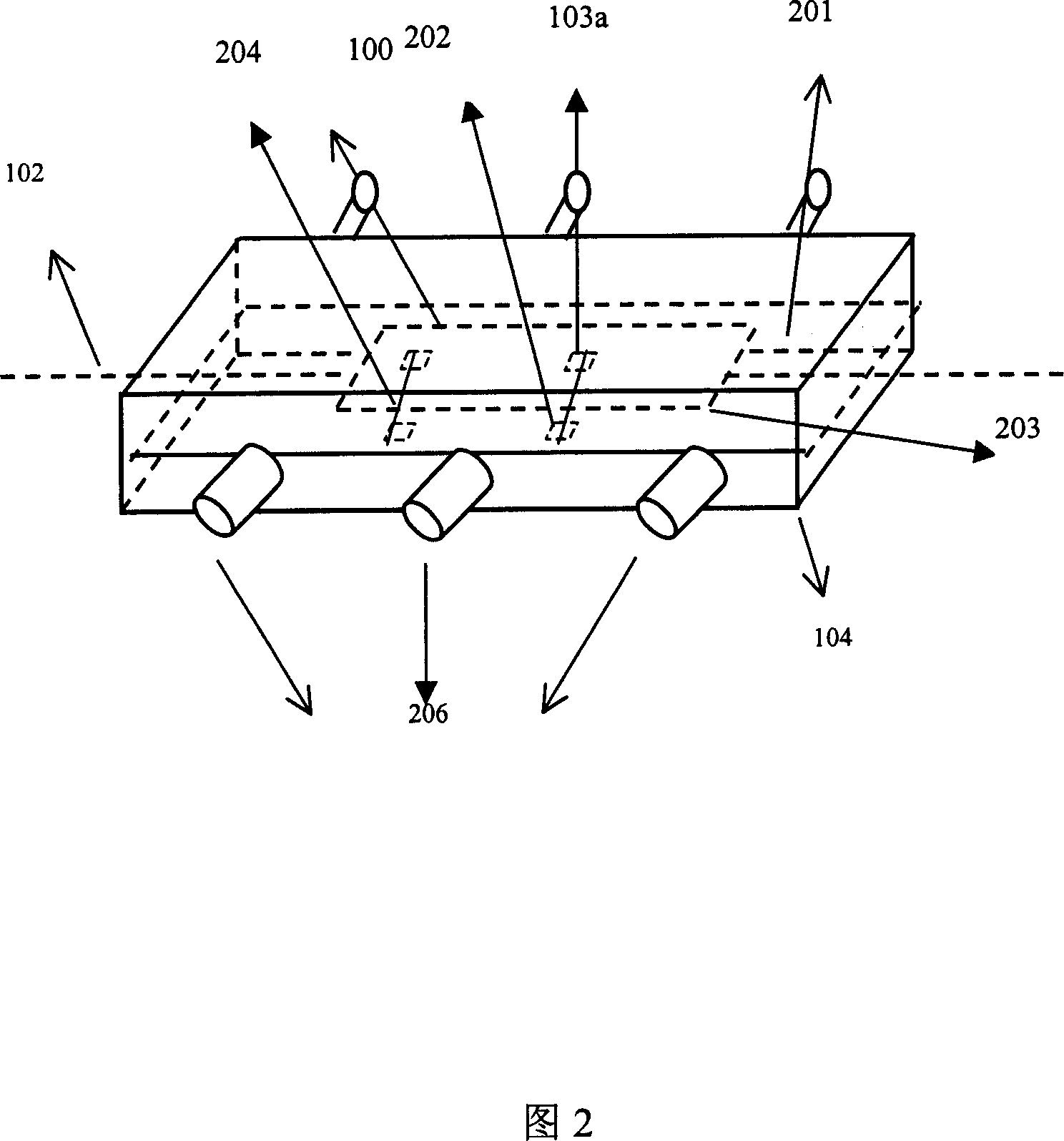
[0049] Please refer to FIG. 2 to FIG. 4 , which show the structure of the selected embodiment of the present invention.
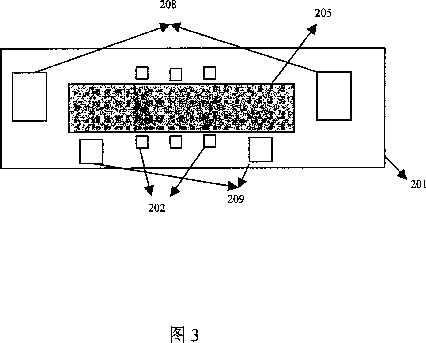
[0050] The present invention relates to a packaging structure of thermo-optic switch array / modulator and its packaging method. The main part of the structure is a printed circuit board with a metal heat dissipation area and a control circuit pattern.
[0051] Figure 2 shows an overall schematic of the package structure. After the thermo-optic switch array / modulator chip 100 is coupled with the optical fiber array 102, it is pasted on the heat dissipation metal area 205 of the printed circuit board 201 by using a colloid with good thermal conductivity and electrical insulation. The drive circuit has been formed on the printed circuit board 201 The pattern, the electrode 103a of the thermo-optic switch array / modulator chip 100 and the output electrode 202 of the printed circuit board are electrically connected by pressure welding, and the control circuit is c...
PUM
 Abstract
Description
Claims
Application Information
 - R&D Engineer
- R&D Manager
- IP Professional
- Industry Leading Data Capabilities
- Powerful AI technology
- Patent DNA Extraction
Browse by: Latest US Patents, China's latest patents, Technical Efficacy Thesaurus, Application Domain, Technology Topic, Popular Technical Reports.
© 2024 PatSnap. All rights reserved.Legal|Privacy policy|Modern Slavery Act Transparency Statement|Sitemap|About US| Contact US: help@patsnap.com