Thinfilm transistor device for reducing leaping voltage

A technology of thin film transistors and devices, which is applied in the field of liquid crystal displays, can solve problems such as crosstalk and picture quality degradation, and achieve the effects of reducing production capacity, increasing process cycle, and improving picture display quality

Active Publication Date: 2007-03-28
BEIJING BOE OPTOELECTRONCIS TECH CO LTD +1
View PDF0 Cites 3 Cited by
  • Summary
  • Abstract
  • Description
  • Claims
  • Application Information

AI Technical Summary

Problems solved by technology

[0010] As mentioned above, the existence of Cgs and ΔVp generated by the overlap between the gate electrode

Method used


Image

  • Thinfilm transistor device for reducing leaping voltage
  • Thinfilm transistor device for reducing leaping voltage
  • Thinfilm transistor device for reducing leaping voltage

Examples


Embodiment Construction

[0026] The present invention will be described in more detail below in conjunction with the accompanying drawings and embodiments.

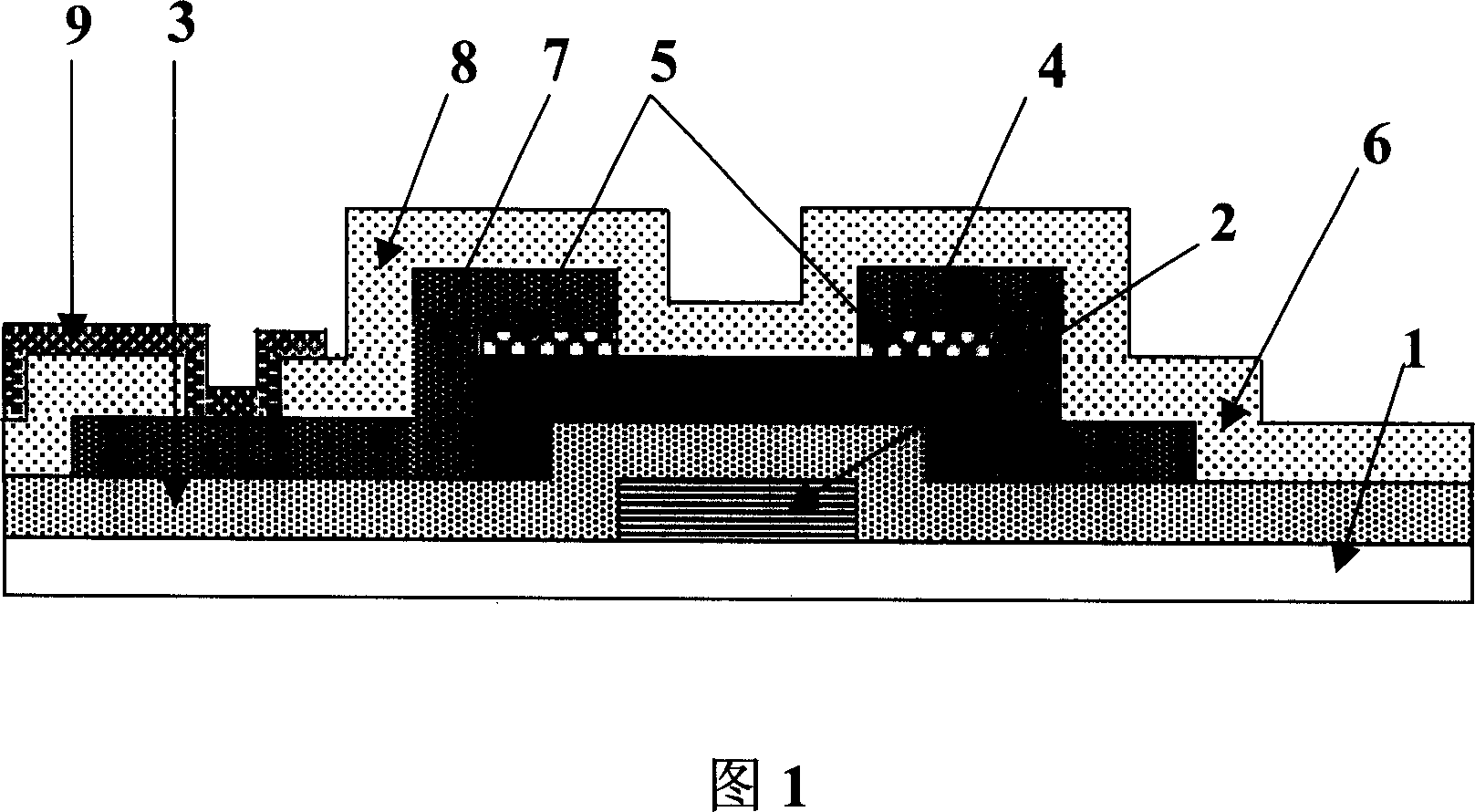
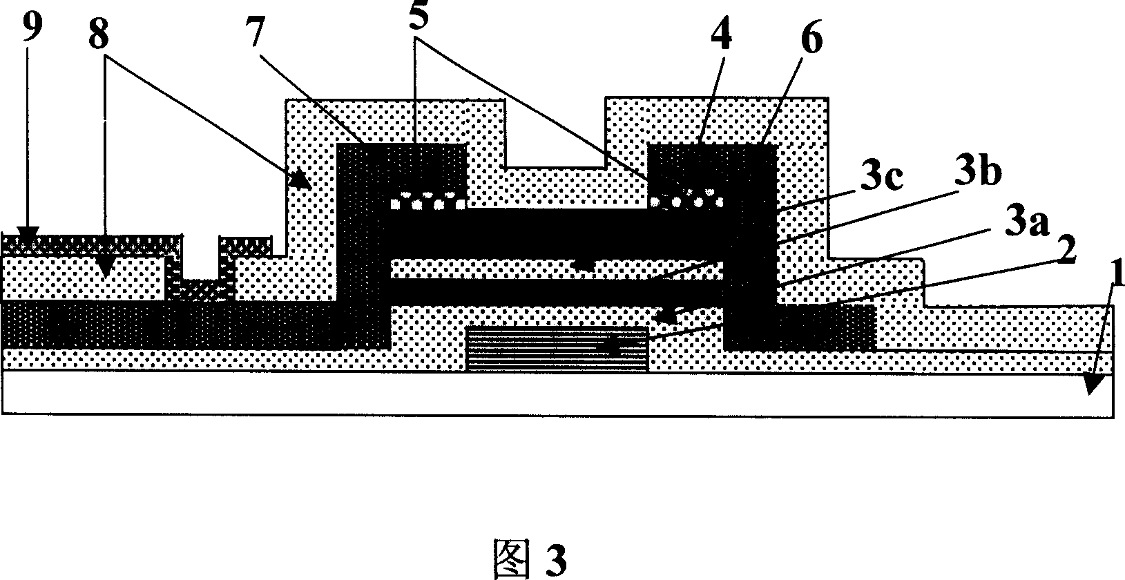
[0027] As shown in Figure 3, the upper and lower films of the gate insulating layer structure under the active layer of the thin film transistor device are silicon nitride, and the intermediate film can be silicon oxide, silicon oxynitride (SiON), fluorine-doped silicon oxide (FSG), carbon-doped silicon oxide (carbon-doped SiO2), silicon nitride (SiC), other doped silicon nitride with low dielectric constant, organic insulating medium with low dielectric constant, etc. Because oxygen-rich silicon oxide (O-rich SiOx) and nitrogen-rich silicon nitride (N-rich SiNx), their dielectric constants have the same variation trend.

[0028] The thickness of the upper layer silicon nitride (etching stop layer) film 3c of the gate insulating layer under the active layer of the thin film transistor is 10 nanometers to 200 nanometers, and the thickness of the l...


PUM

PropertyMeasurementUnit
Thicknessaaaaaaaaaa
Thicknessaaaaaaaaaa
Thicknessaaaaaaaaaa

Abstract

The thin film transistor device includes following parts: a transparent glass base plate; gate electrode; insulating layer of gate electrode for partitioning scan line of gate electrode from scan line of source electrode; active layer, doping layer; source/drain electrodes; passivation layer for partitioning scan line of source electrode from transparent pixel electrode. Gate insulating layer under the active layer includes three layers of insulating medium. Dielectric constant of middle insulating-film is lower than Dielectric constants of insulating-film at upper layer and insulating-film at lower layer. Thus, the device possesses lower leaping voltage so as to restrain flicker and crosstalk on liquid crystal display of using the thin film transistor as well as improve quality of displayed images.

Description

technical field [0001] This patent relates to a thin film transistor of a liquid crystal display panel, especially a structure for reducing jump voltage by controlling parasitic capacitance, which belongs to the field of liquid crystal display. Background technique [0002] Over the past decade, liquid crystal displays have attracted increasing attention as a flat panel display technology. It is characterized by small size and portability, and compared with traditional cathode ray tubes and other flat panel displays (such as plasma displays), LCD displays consume less power. In particular, TFT-LCD devices are widely used in office equipment and home imaging equipment. TFT-LCD devices control each pixel to obtain different driving voltages through thin film transistors, so as to realize the display of fine images. [0003] FIG. 1 shows a cross-section of a thin film transistor in a single pixel in a prior art TFT-LCD device. The usual manufacturing process is: [0004] Fi...

Claims


Application Information

Patent Timeline
IPC IPC(8): H01L29/786H01L27/12G02F1/1368
Inventor 龙春平邓朝永林承武
Owner BEIJING BOE OPTOELECTRONCIS TECH CO LTD
Why Eureka
Try Eureka