Inductive coupling source
An inductive coupling and inductive coupling coil technology, applied in the field of microelectronics, can solve the problems of unstable impedance matching, excessive inductance, low coupling efficiency, etc., and achieve the effects of superior performance, reduced dependence, and uniform magnetic field strength
- Summary
- Abstract
- Description
- Claims
- Application Information
AI Technical Summary
Problems solved by technology
Method used
Image

Examples
Embodiment Construction
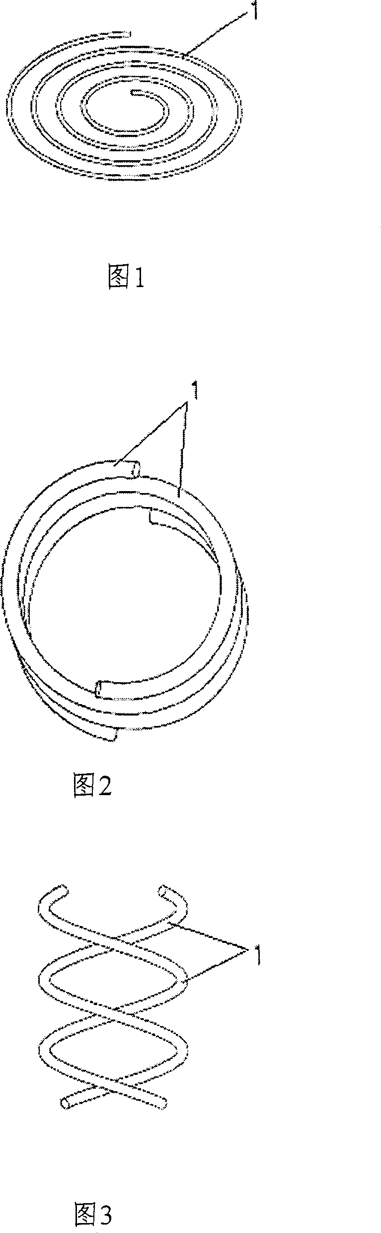
[0027] The specific implementation manner of the inductive coupling source of the present invention will be further described in detail below in conjunction with the accompanying drawings, but it is not used to limit the protection scope of the present invention.
[0028] See Figures 2 through 4. The structure of the first embodiment of the inductively coupled source of the present invention includes a pair of inductively coupled coils 1 and excitation sources that are nested and arranged in complete symmetry. The inductively coupled coil is an involute multi-turn three-dimensional coil. The excitation source is a radio frequency power source.
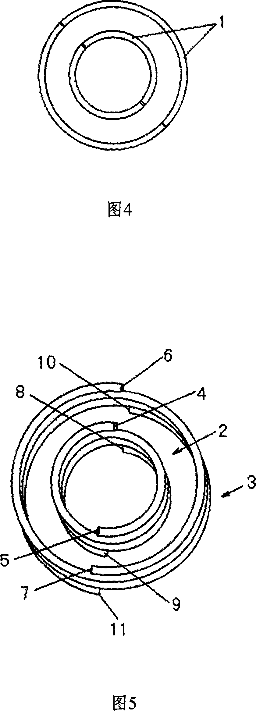
[0029] See Figure 5. The structure of the second embodiment of the inductively coupled source of the present invention includes an inner group coil 2 and an outer group coil 3 and an excitation source connected in series or together, wherein the inner group coil 2 and the outer group coil 3 are each formed of a pair of completely sym...
PUM
 Abstract
Description
Claims
Application Information
 - R&D
- Intellectual Property
- Life Sciences
- Materials
- Tech Scout
- Unparalleled Data Quality
- Higher Quality Content
- 60% Fewer Hallucinations
Browse by: Latest US Patents, China's latest patents, Technical Efficacy Thesaurus, Application Domain, Technology Topic, Popular Technical Reports.
© 2025 PatSnap. All rights reserved.Legal|Privacy policy|Modern Slavery Act Transparency Statement|Sitemap|About US| Contact US: help@patsnap.com