Condensing element and solid state imaging device
A technology of solid-state imaging device and light-gathering element, which is applied in the directions of optical components, electrical components, and electric solid-state devices, etc., can solve the problems of application difficulty, reduction, and low pixel light-gathering efficiency.
- Summary
- Abstract
- Description
- Claims
- Application Information
AI Technical Summary
Problems solved by technology
Method used
Image

Examples
Embodiment approach 1
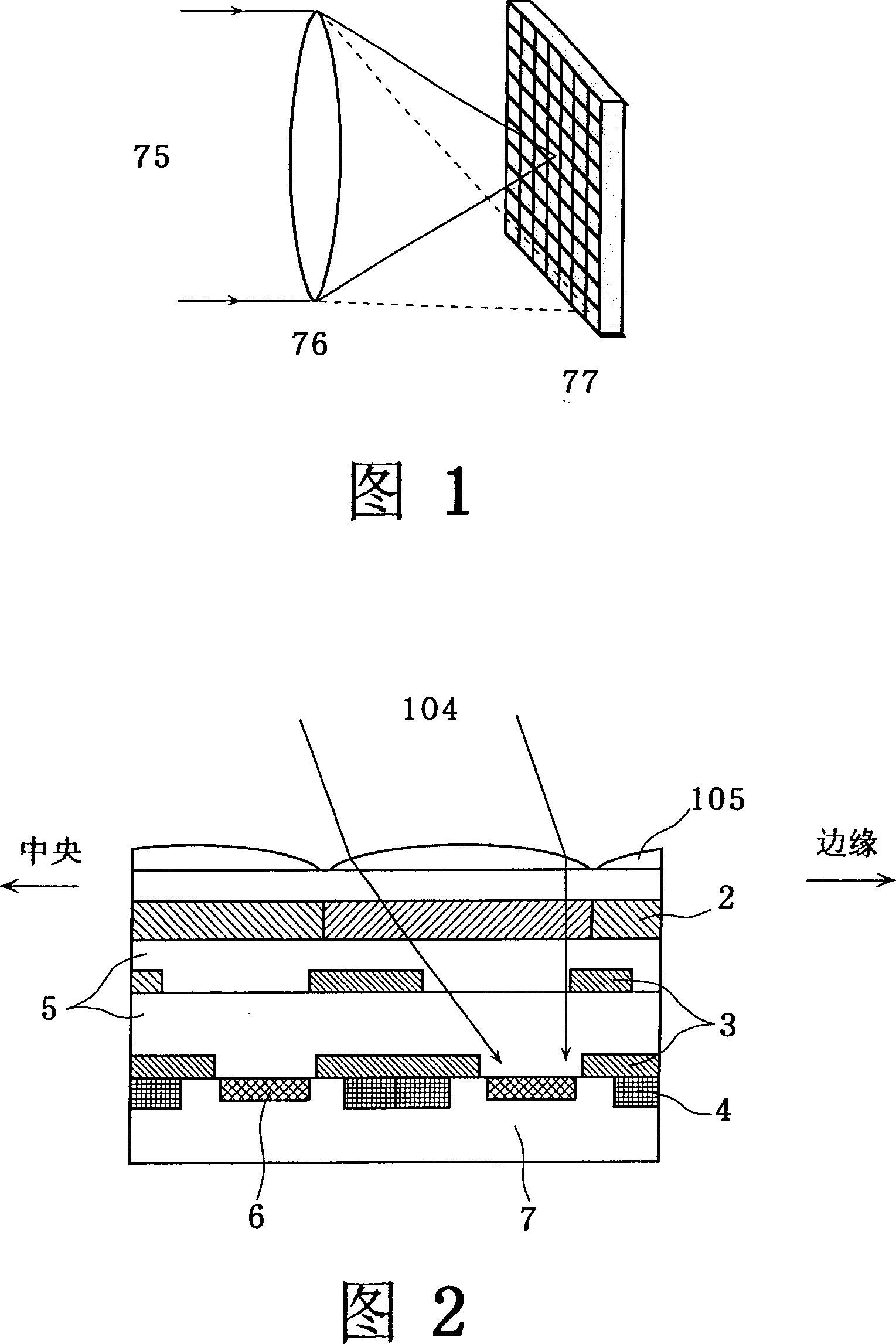
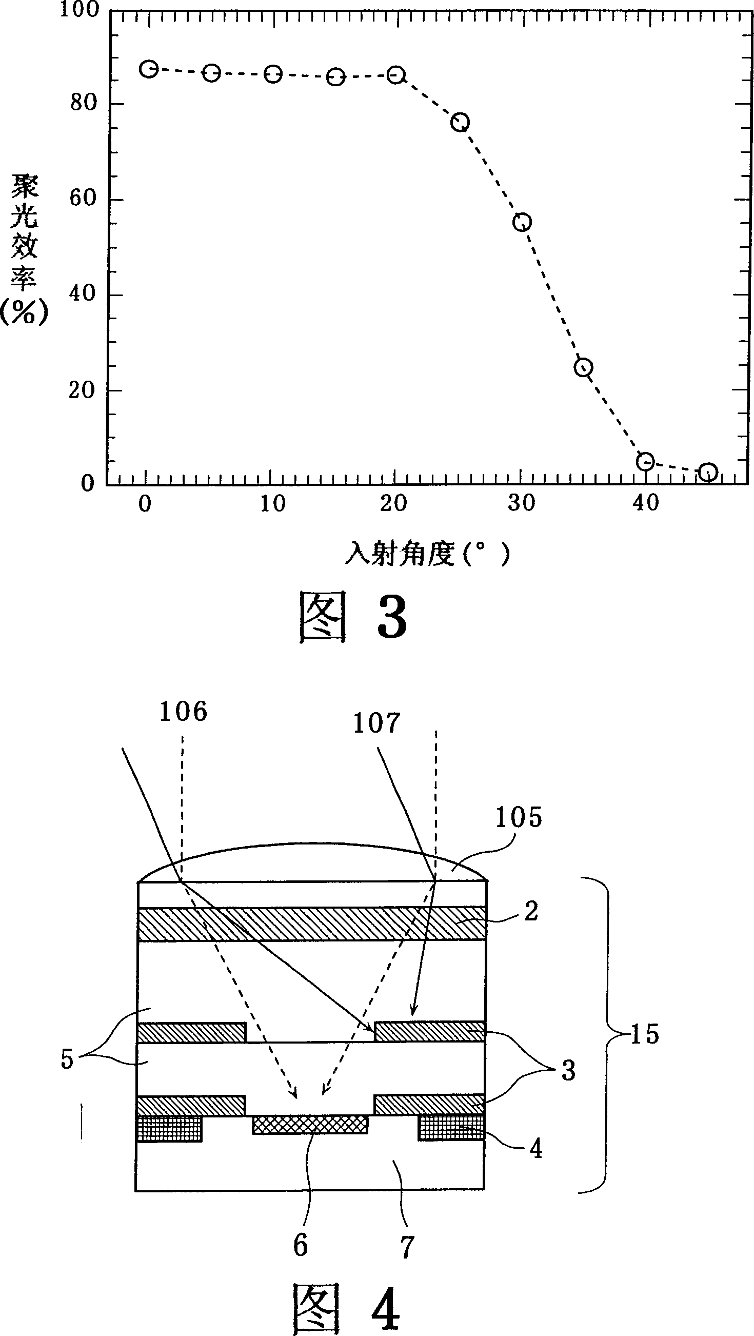
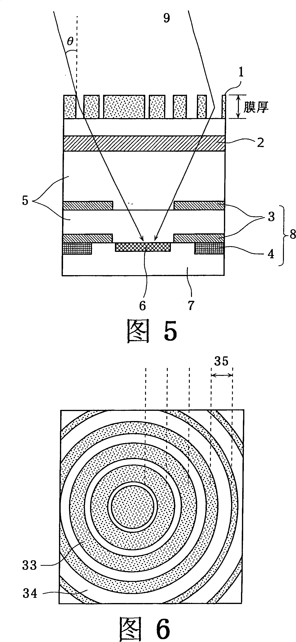
[0192]FIG. 5 is a diagram showing a basic configuration of a solid-state imaging device according to this embodiment. Each pixel (2.8 μm in size) includes: a graded-index lens (also referred to as “aggregate of light-transmitting films”) 1, a color filter for green 2, an AL line 3, a signal transmission unit 4, and a flattening layer 5 , a light-receiving element (silicon photodiode) 6 , and a silicon substrate 7 . Fig. 6 is a plan view showing a graded-index lens.
[0193] The concentric circle structure of this graded index lens 1 comprises high refractive index material 33 [TiO 2 (n=2.53)] and low-refractive index material 34 [air (n=1.0)], and have a plurality of division areas, the width 35 of this division area is made up of adjacent 2 areas, such as this width is certain, The value is 200nm. In addition, the film thickness t was 0.5 μm.
[0194] As shown in FIG. 6 , each light-transmitting film has a band shape, a centrosymmetric shape deviated from the center, and ...
Embodiment approach 2
[0224] 12( a ) to ( c ) are photographs taken under a scanning electron microscope (SEM) of a graded-index lens having a concentric circular structure in Embodiment 2 of the present invention. This graded-index lens is formed on a fused silica substrate by drawing with an electron beam (EB: electron beam). Specifically, this graded-index lens uses a resist film (ZEP520: Refractive Index 1.56) and the refractive index difference of air. The detailed production method will be described later. The lens diameter is 2.8 μm, the lens thickness is 1 μm, and the width of the divided region is 0.2 μm. The refractive index distribution is designed according to the above formula (5), with a focal length of 5 μm, a wavelength of incident light of 0.55 μm, a refractive index of the incident side medium of 1.45 (fused silica), and a refractive index of the exit side medium of 1 (air).
[0225] Fig. 12(a) is a top view photo of a graded-index lens with an incident angle setting value of 0°...
Embodiment approach 3
[0233] 17( a ) to ( c ) are diagrams showing a basic configuration of one pixel according to Embodiment 3. FIG. The lens related to this pixel imparts the phase modulation of the above formula (4) to incident light, and has a refractive index distribution in a single Fresnel zone region. Incident light 66 is incident to the entrance window at an incident angle of 0°, and is condensed by a gradient index lens 69 for incident light at 0°; incident light 67 is incident to the entrance window at an incident angle of α / 2°, and passes through GRIN lens 70 for α / 2° incident light to condense light; and incident light 68, incident to the entrance window at an incident angle α°, and condensed by GRIN lens 71 for α° incident light ; Through the color filter 2, it is converted into an electrical signal in the light receiving part. Here, the angle α is defined by the following formula (8). Here, D is the pixel size.
[0234] [Formula 14]
[0235] α = ...
PUM
 Abstract
Description
Claims
Application Information
 - R&D Engineer
- R&D Manager
- IP Professional
- Industry Leading Data Capabilities
- Powerful AI technology
- Patent DNA Extraction
Browse by: Latest US Patents, China's latest patents, Technical Efficacy Thesaurus, Application Domain, Technology Topic.
© 2024 PatSnap. All rights reserved.Legal|Privacy policy|Modern Slavery Act Transparency Statement|Sitemap